Toggle light / dark theme

Here’s a new chapter in the story of the miniaturisation of machines: researchers in a laboratory in Singapore have shown that a single atom can function as either an engine or a fridge. Such a device could be engineered into future computers and fuel cells to control energy flows.

“Think about how your computer or laptop has a lot of things inside it that heat up. Today you cool that with a fan that blows air. In nanomachines or quantum computers, small devices that do cooling could be something useful,” says Dario Poletti from the Singapore University of Technology and Design (SUTD).

This work gives new insight into the mechanics of such devices. The work is a collaboration involving researchers at the Centre for Quantum Technologies (CQT) and Department of Physics at the National University of Singapore (NUS), SUTD and at the University of Augsburg in Germany. The results were published in the peer-reviewed journal npj Quantum Information on 1 May.

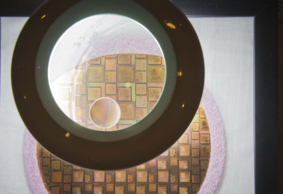
Tiny integrated circuits destined for space missions, etched onto a single wafer of silicon, examined under a magnifier.

To save money on the high cost of fabrication, various chips designed by different companies and destined for multiple ESA projects are crammed onto the same silicon wafers, etched into place at specialised semiconductor manufacturing plants or ‘fabs’.

Once manufactured, the chips, still on the wafer, are tested. The wafers are then chopped up. They become ready for use when placed inside protective packages – just like standard terrestrial microprocessors – and undergo final quality tests.

At the Paul Scherrer Institute PSI, researchers have gained insights into a promising material for organic light-emitting diodes (OLEDs). The substance enables high light yields and would be inexpensive to produce on a large scale—that means it is practically made for use in large-area room lighting. Researchers have been searching for such materials for a long time. The newly generated understanding will facilitate the rapid and cost-efficient development of new lighting appliances in the future. The study appears today in the journal Nature Communications.

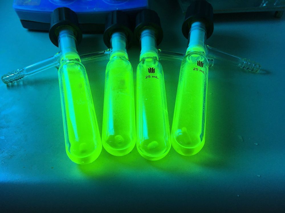
The compound is a yellowish solid. If you dissolve it in a liquid or place a of it on an electrode and then apply an , it gives off an intense green glow. The reason: The molecules absorb the energy supplied to them and gradually emit it again in the form of light. This process is called electroluminescence. Light-emitting diodes are based on this principle.

This green luminescent substance is a hot candidate for producing OLEDs, -emitting diodes. For about three years now, OLEDs have been found in the displays of smartphones, for example. In the meantime, the first flexible television screens with these materials have also come onto the market.

Army researchers predict quantum computer circuits that will no longer need extremely cold temperatures to function could become a reality after about a decade.

For years, solid-state quantum technology that operates at room temperature seemed remote. While the application of transparent crystals with had emerged as the most likely route to this milestone, the plausibility of such a system always remained in question.

Now, Army scientists have officially confirmed the validity of this approach. Dr. Kurt Jacobs, of the U.S. Army Combat Capabilities Development Command’s Army Research Laboratory, working alongside Dr. Mikkel Heuck and Prof. Dirk Englund, of the Massachusetts Institute of Technology, became the first to demonstrate the feasibility of a quantum logic gate comprised of and optical crystals.

To tackle this problem, researchers at the RIKEN Center for Biosystems Dynamics Research identified a gel that closely mimics the physicochemical properties of organs that have undergone the tissue clearing process. Starting with computer simulations and following up with laboratory tests, the team optimized the soaking solution temperature, dye and antibody concentrations, chemical additives, and electrical properties to produce the best staining and imaging results. They then tested their method with more than two dozen commonly used dyes and antibodies on mouse and marmoset brains.

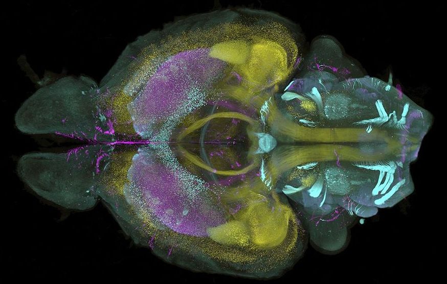
Scans of an entire mouse brain and one hemisphere of a marmoset brain—rendered into 3D using light sheet microscopy—revealed the similarity between the two animals’ neural vascular systems, showing the use of the system for comparative anatomy, the researchers report this week in. They also showed that they could simultaneously stain and image up to four molecular targets in a mouse brain, a feat that “has never been reported before,” says Ludovico Silvestri, of the European Laboratory for Non-linear Spectroscopy, who was not involved in the research.

The team also used its technique to image an entire infant marmoset and a small human brain sample—something that could one day lead to new understandings of solid tumors and neurodegenerative diseases. The team says its approach to optimizing staining can be applied to other techniques to advance the entire field of 3D imaging.

Researchers at Stanford University have recently carried out an in-depth study of nematic transitions in iron pnictide superconductors. Their paper, published in Nature Physics, presents new imaging data of these transitions collected using a microscope they invented, dubbed the scanning quantum cryogenic atom microscope (SQCRAMscope).

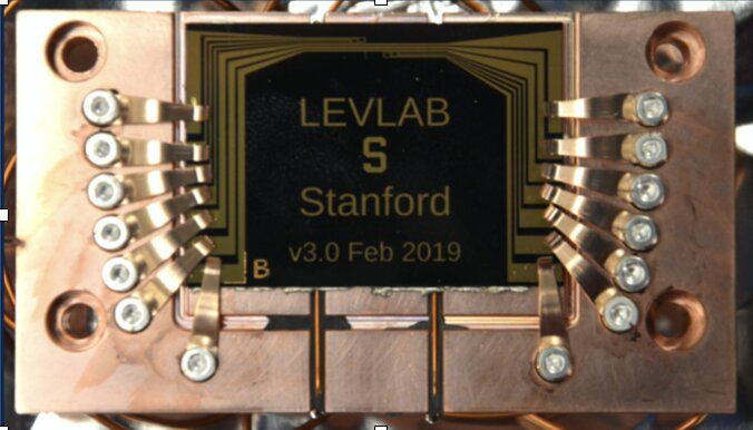
“We invented a new type of scanning probe microscope a few years ago,” Benjamin L. Lev, the researcher who led the study, told Phys.org. “One can think of it like a normal optical microscope, but instead of the lens focused on some sample slide, the focus is on a quantum gas of atoms that are levitated near the sample.”

In the new microscope invented by Lev and his colleagues, atoms are levitated from an ‘atom chip’ trapping device using magnetic fields, until they are merely a micron above the sample slide. These atoms can transduce the magnetic fields that emanate from the sample into the light collected by the microscope’s lens. As a result, SQCRAMscope can be used to image magnetic fields.

DisplayPort Alt Mode 2.0 is a new standard from the Video Electronics Standards Association that allows USB 4 to offer all the bells and whistles of the DisplayPort 2.0 standard as well as transmitting USB data. That means support for 8K displays at 60Hz with HDR, 4K displays at 144Hz with HDR, or even 16K (15360×8460) displays at 60Hz with compression. It’s a big step towards USB Type-C becoming a true jack-of-all trades connector.

The USB 4 spec can already transmit DisplayPort data, but AnandTech reports that the new standard remaps USB-C’s high speed data pins to unlock more bandwidth for video. USB 4 is bidirectional, meaning it can carry up to 40Gbps of data in either direction. However, video doesn’t need to go both ways — you only really need data to pass from your laptop to your monitor (for example). This alt mode means that all that bandwidth can be used to just send video one way, meaning you get a maximum raw bandwidth of up to 80Gbps.

Today’s virtual reality systems can create immersive visual experiences, but seldom do they enable users to feel anything—particularly walls, appliances and furniture. A new device developed at Carnegie Mellon University, however, uses multiple strings attached to the hand and fingers to simulate the feel of obstacles and heavy objects.

By locking the strings when the user’s hand is near a virtual wall, for instance, the device simulates the sense of touching the wall. Similarly, the string mechanism enables people to feel the contours of a virtual sculpture, sense resistance when they push on a piece of furniture or even give a high five to a virtual character.

Cathy Fang, who will graduate from CMU next month with a joint degree in mechanical engineering and , said the shoulder-mounted device takes advantage of spring-loaded strings to reduce weight, consume less battery power and keep costs low.

Scientists typically use a method known as polymerase chain reaction (PCR), but it requires bulky and expensive equipment and considerable expertise to perform correctly. That means DNA samples collected in the field normally have to be sent to dedicated laboratories for testing, which makes it hard to detect diseases or harmful pathogens quickly.

A new testing system developed by researchers at the Army Medical University in China may help to fill that gap by allowing on-the-spot DNA tests in as quick as 80 minutes. According to the researchers, their test achieves 97 percent accuracy using simple 3D printed parts that attach to a standard smartphone and weigh less than 100 g rams (0.22 pounds).

At the heart of the system is an “i-chip” just four centimeters long that includes integrated sample preparation, DNA amplification, and signal detection modules. The various reagents required to carry out the test can be pre-loaded in the device, and the researchers showed that these could be kept for up to ten weeks at room temperature without loss of performance.