Toggle light / dark theme

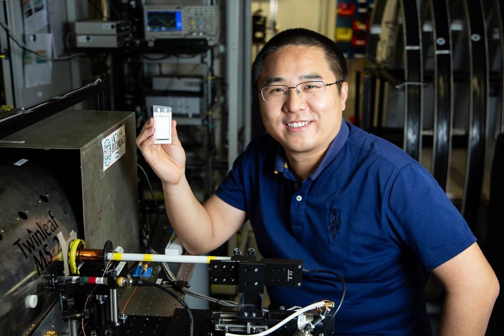
Rechargeable batteries are at the heart of many new technologies involving, for example, the increased use of renewable energies. More specifically, they are employed to power electric vehicles, cell phones, and laptops. Scientists at Johannes Gutenberg University Mainz (JGU) and the Helmholtz Institute Mainz (HIM) in Germany have now presented a non-contact method for detecting the state of charge and any defects in lithium-ion batteries. For this purpose, atomic magnetometers are used to measure the magnetic field around battery cells. Professor Dmitry Budker and his team usually use atomic magnetometry to explore fundamental questions of physics, such as the search for new particles. Magnetometry is the term used to describe the measurement of magnetic fields. One simple example of its application is the compass, which the Earth’s magnetic field causes to point north.

Non-contact quality assurance of batteries using atomic magnetometers

The demand for high-capacity is growing and so is the need for a form of sensitive, accurate diagnostic technology for determining the state of a battery cell. The success of many new developments will depend on whether batteries can be produced that can deliver sufficient capacity and a long effective life span. “Undertaking the quality assurance of rechargeable batteries is a significant challenge. Non-contact methods can potentially provide fresh stimulus for improvement in batteries,” said Dr. Arne Wickenbrock, a member of Professor Dmitry Budker’s work group at the JGU Institute of Physics and the Helmholtz Institute Mainz. The group has achieved a breakthrough by using atomic magnetometers to take measurements. The idea came about during a teleconference between Budker and his colleague Professor Alexej Jerschow of New York University. They developed a concept and, with close cooperation between the two groups, carried out the related experiments in Mainz.
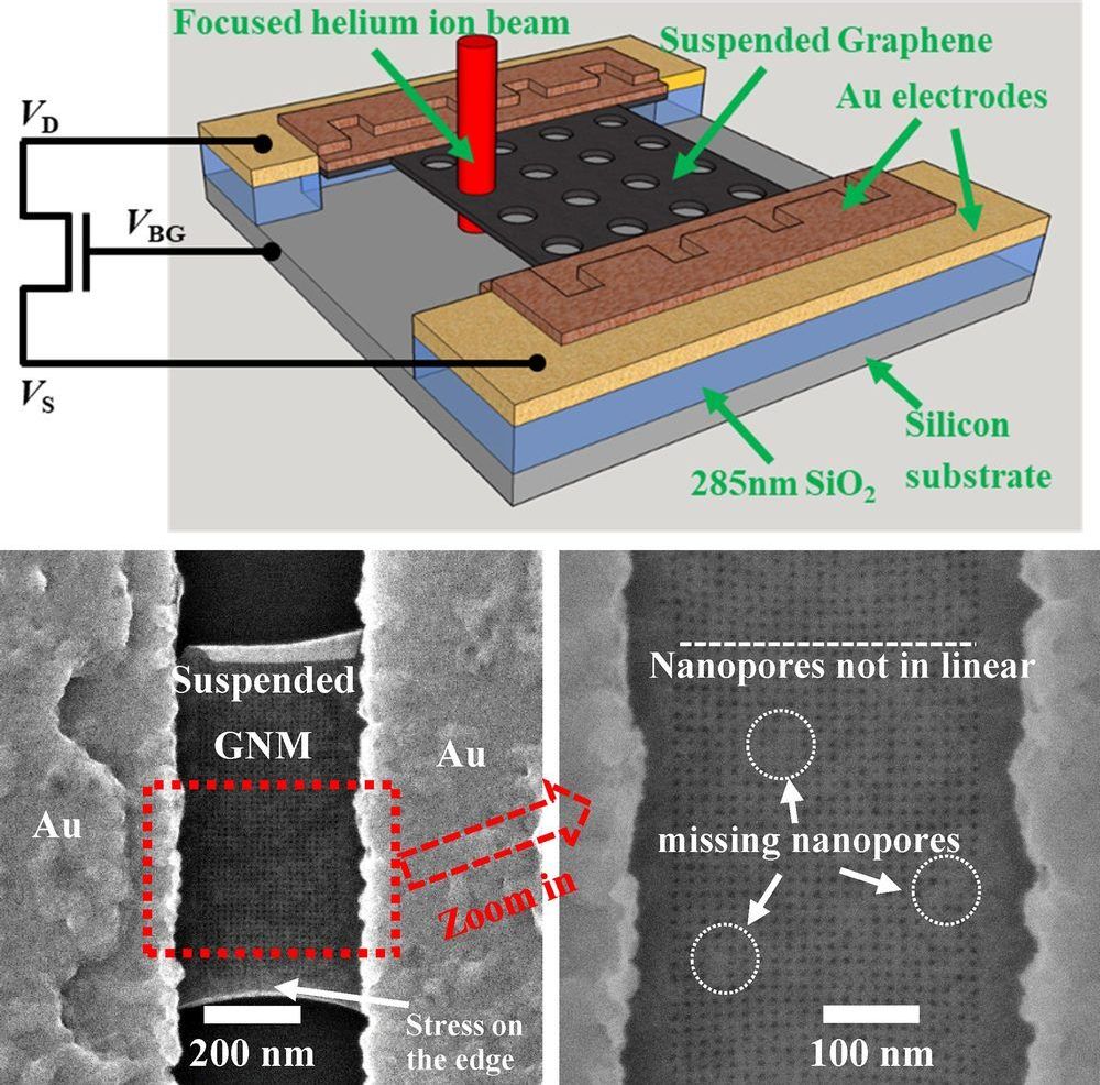
Researchers at Japan advanced institute of science and technology (JAIST) have successfully fabrication the suspended graphene nanomesh in a large area by the helium ion beam microscopy. 6nm diameter nanopores were pattern on the 1.2 um long and 500 nm wide suspended graphene uniformly. By systematically controlling the pitch (nanopore’s center to nanopore’s center) from 15 nm to 50 nm, a series of stable graphene nanomesh devices were achieved. This provides a practical way to investigate the intrinsic properties of graphene nanomesh towards the application for gas sensing, phonon engineering, and quantum technology.

Graphene, with its excellent electrical, thermal and optical properties, is promising for many applications in the next decade. It is also a potential candidate instead of silicon to build the next generation of electrical circuits. However, without a bandgap, it is not straightforward to use graphene as field-effect transistors (FETs). Researchers tried to cut the graphene sheet into a small piece of graphene nanoribbon and observed the bandgap opening successfully. However, the current of graphene nanoribbons is too low to drive the integrated circuit. In this case, the graphene nanomesh is pointed out by introducing periodical nanopores on the graphene, which is also considered as very small graphene nanoribbon array.

A research team led by Dr Fayong Liu and Professor Hiroshi MIZUTA has demonstrated in collaboration with researchers at the National Institute of Advanced Industrial Science and Technology (AIST) that large area suspended graphene nanomesh is quickly achievable by the helium ion beam microscopy with sub-10 nm nanopore diameter and well-controlled pitches. Comparing to slow speed TEM patterning, the helium ion beam milling technique overcomes the speed limitation, and meanwhile, provides a high imaging resolution. With the initial electrical measurements, it has found that the thermal activation energy of the graphene nanomesh increased exponentially by increasing the porosity of the graphene nanomesh. This immediately provides a new method for bandgap engineering beyond the conventional nanoribbon method. The team plans to continue exploring graphene nanomesh towards the application of phonon engineering.

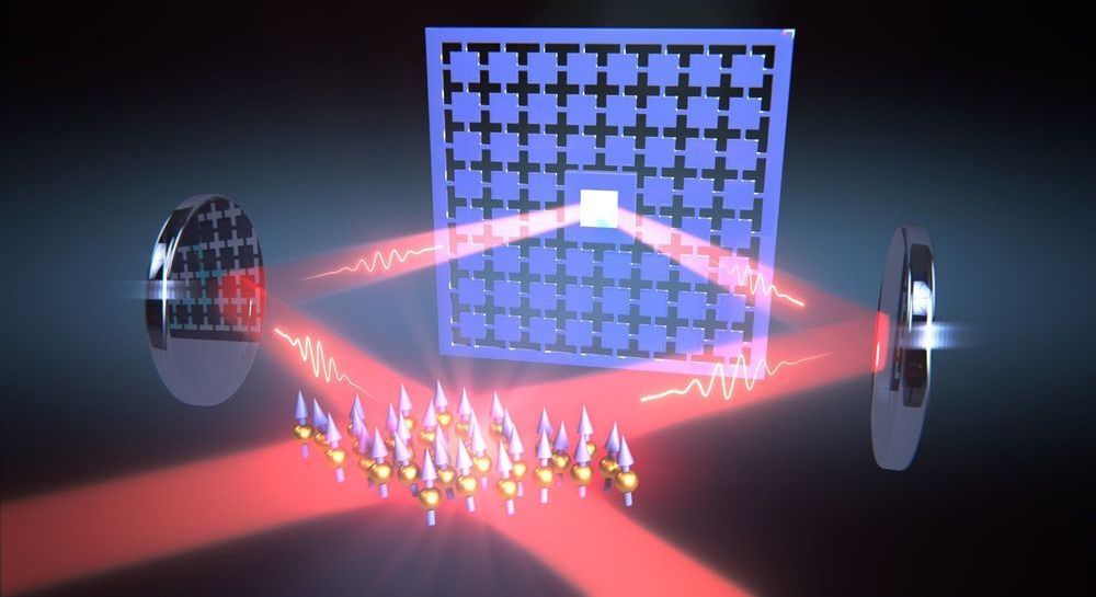
For the first time, researchers have succeeded in creating strong coupling between quantum systems over a great distance. They accomplished this with a novel method in which a laser loop connects the systems, enabling nearly lossless exchange of information and strong interaction between them. In the journal Science, physicists from the University of Basel and University of Hanover reported that the new method opens up new possibilities in quantum networks and quantum sensor technology.

Quantum technology is currently one of the most active fields of research worldwide. It takes advantage of the special properties of quantum mechanical states of atoms, light, or nanostructures to develop, for example, novel sensors for medicine and navigation, networks for information processing and powerful simulators for materials sciences. Generating these quantum states normally requires a between the systems involved, such as between several atoms or nanostructures.

Until now, however, sufficiently strong interactions were limited to short distances. Typically, two systems had to be placed close to each other on the same chip at low temperatures or in the same vacuum chamber, where they interact via electrostatic or magnetostatic forces. Coupling them across larger distances, however, is required for many applications such as or certain types of sensors.

Quantum computing is seen by many as a technology of the future. In this article, we’re going to look at how to run some non-trivial programs on actual quantum computers. In particular, we’re going to discuss something called graph states. Graph states are used for quantum cryptography, quantum error correction, and measurement based quantum computing. If all of that sounds like a foreign language, that’s okay. We’re going to go through everything, from the ground up, and in detail…and don’t worry, we’ll keep it light and fun.

Princeton researchers detect a supercurrent a current flowing without energy loss at the edge of a superconductor with a topological twist.

A discovery that long eluded physicists has been detected in a laboratory at Princeton. A team of physicists detected superconducting currents — the flow of electrons without wasting energy — along the exterior edge of a superconducting material. The finding was published May 1 in the journal Science.

The superconductor that the researchers studied is also a topological semi-metal, a material that comes with its own unusual electronic properties. The finding suggests ways to unlock a new era of “topological superconductivity” that could have value for quantum computing.

Circa 2015


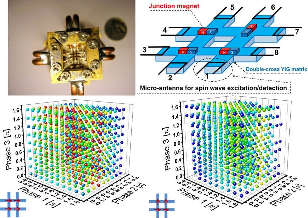
Researchers at the University of California, Riverside Bourns College of Engineering and the Russian Academy of Sciences have successfully demonstrated pattern recognition using a magnonic holographic memory device, a development that could greatly improve speech and image recognition hardware.

Pattern recognition focuses on finding patterns and regularities in data. The uniqueness of the demonstrated work is that the input patterns are encoded into the phases of the input spin waves.

Spin waves are collective oscillations of spins in magnetic materials. Spin wave devices are advantageous over their optical counterparts because they are more scalable due to a shorter wavelength. Also, spin wave devices are compatible with conventional electronic devices and can be integrated within a chip.

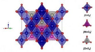
Spinels are oxides with chemical formulas of the type AB2O4, where A is a divalent metal cation (positive ion), B is a trivalent metal cation, and O is oxygen. Spinels are valued for their beauty, which derives from the molecules’ spatial configurations, but spinels in which the trivalent cation B consists of the element chrome (Cr) are interesting for a reason that has nothing to do with aesthetics: They have magnetic properties with an abundance of potential technological applications, including gas sensors, drug carriers, data storage media, and components of telecommunications systems.

A study by Brazilian and Indian researchers investigated a peculiar kind of spinel: zinc-doped manganese chromite. Nanoparticles of this material, described by the formula Mn0.5 Zn0.5 Cr2O4 [where manganese (Mn) and zinc (Zn) compose the A-site divalent cation], were synthesized in the laboratory and characterized by calculations based on density functional theory (DFT), a method derived from that is used in solid-state physics and chemistry to resolve complex crystal structures.

The material’s structural, electronic, vibrational and were determined by X-ray diffraction, neutron diffraction, X-ray photoelectron spectroscopy and Raman spectroscopy. A report of the study has been published in the Journal of Magnetism and Magnetic Materials with the title “Structural, electronic, vibrational and magnetic properties of Zn2+ substituted MnCr2O4 nanoparticles.”

Circa 2018


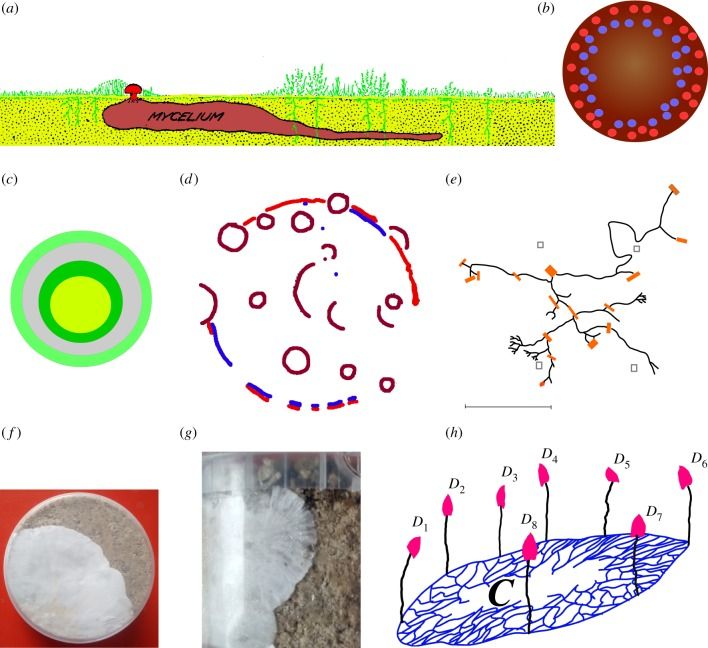
We propose that fungi Basidiomycetes can be used as computing devices: information is represented by spikes of electrical activity, a computation is implemented in a mycelium network and an interface is realized via fruit bodies. In a series of scoping experiments, we demonstrate that electrical activity recorded on fruits might act as a reliable indicator of the fungi’s response to thermal and chemical stimulation. A stimulation of a fruit is reflected in changes of electrical activity of other fruits of a cluster, i.e. there is distant information transfer between fungal fruit bodies. In an automaton model of a fungal computer, we show how to implement computation with fungi and demonstrate that a structure of logical functions computed is determined by mycelium geometry.

The fungi are the largest, widely distributed and oldest group of living organisms [1]. The smallest fungi are microscopic single cells. The largest mycelium belongs to Armillaria bulbosa, which occupies 15 hectares and weights 10 tons [2], and the largest fruit body belongs to Fomitiporia ellipsoidea, which at 20 years old is 11 m long, 80 cm wide, 5 cm thick and has an estimated weight of nearly half-a-ton [3]. During the last decade, we produced nearly 40 prototypes of sensing and computing devices from the slime mould Physarum polycephalum [4], including the shortest path finders, computational geometry processors, hybrid electronic devices, see the compilation of the latest results in [5].

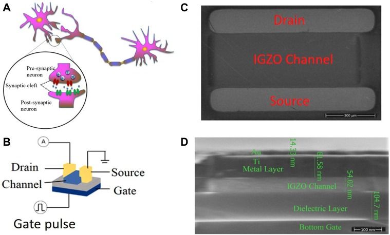
Electronic devices which mimic the functionality of biological synapses are a large step to replicate the human brain for neuromorphic computing and for numerous medical research investigations. One of the representative synaptic behaviors is paired-pulse facilitation (PPF). It has been widely investigated because it is regarded to be related to biological memory. However, plasticity behavior is only part of the human brain memory behavior.

Here, we present a phenomenon which is opposite to PPF, i.e., paired-pulse inhibition (PPI), in nano oxide devices for the first time. The research here suggests that rather than being enhanced, the phenomena of memory loss would also be possessed by such electronic devices. The device physics mechanism behind memory loss behavior was investigated. This mechanism is sustained by historical memory and degradation manufactured by device trauma to regulate characteristically stimulated origins of artificial transmission behaviors.

Under the trauma of a memory device, both the signal amplitude and signal time stimulated by a pulse are lower than the first signal stimulated by a previous pulse in the PPF, representing a new scenario in the struggle for memory. In this way, more typical human brain behaviors could be simulated, including the effect of age on latency and error generation, cerebellar infarct, trauma and memory loss pharmacological actions (such as those caused by hyoscines and nitrazepam).