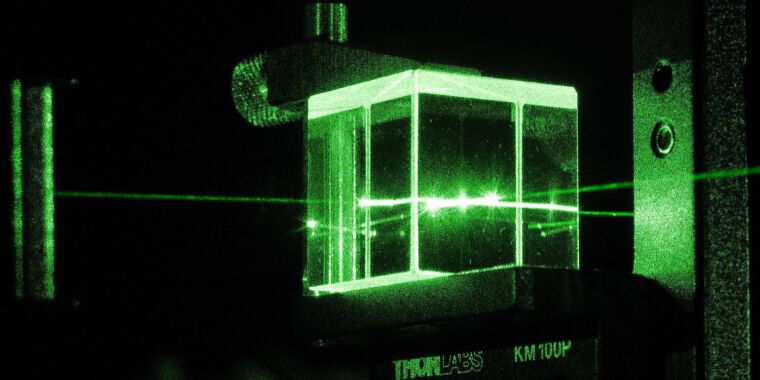
Photons explore quantum maze faster than possible for any classical computer.


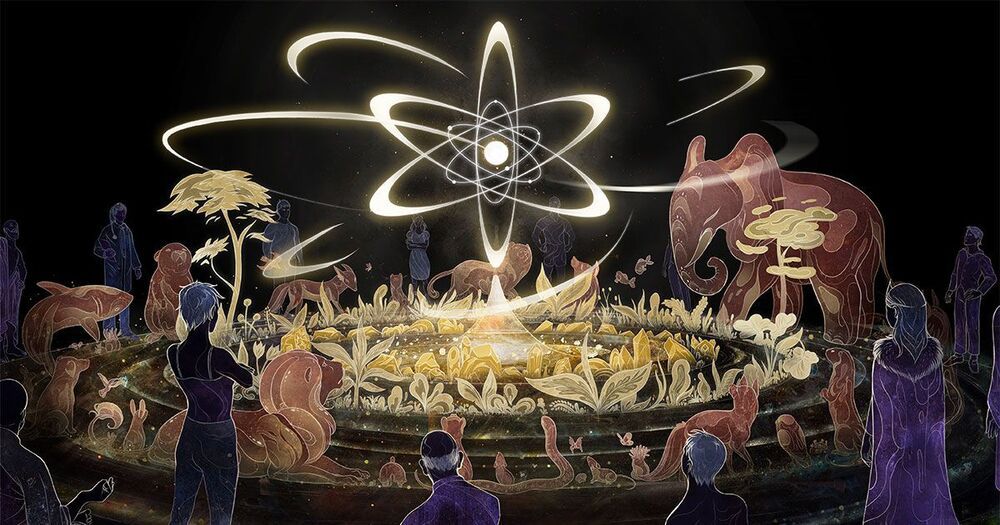

Scientists discovered a strategy for layering dissimilar crystals with atomic precision to control the size of resulting magnetic quasi-particles called skyrmions. This approach could advance high-density data storage and quantum magnets for quantum information science.
In typical ferromagnets, magnetic spins align up or down. Yet in skyrmions, they twist and swirl, forming unique shapes like petite porcupines or tiny tornadoes.
The tiny intertwined magnetic structures could innovate high-density data storage, for which size does matter and must be small. The Oak Ridge National Laboratory-led project produced skyrmions as small as 10 nanometers – 10,000 times thinner than a human hair.


Understanding how matter interacts with light—its optical properties—is critical in a myriad of energy and biomedical technologies, such as targeted drug delivery, quantum dots, fuel combustion, and cracking of biomass. But calculating these properties is computationally intensive, and the inverse problem—designing a structure with desired optical properties—is even harder.
Now Berkeley Lab scientists have developed a machine learning model that can be used for both problems—calculating optical properties of a known structure and, inversely, designing a structure with desired optical properties. Their study was published in Cell Reports Physical Science.
“Our model performs bi-directionally with high accuracy and its interpretation qualitatively recovers physics of how metal and dielectric materials interact with light,” said corresponding author Sean Lubner.
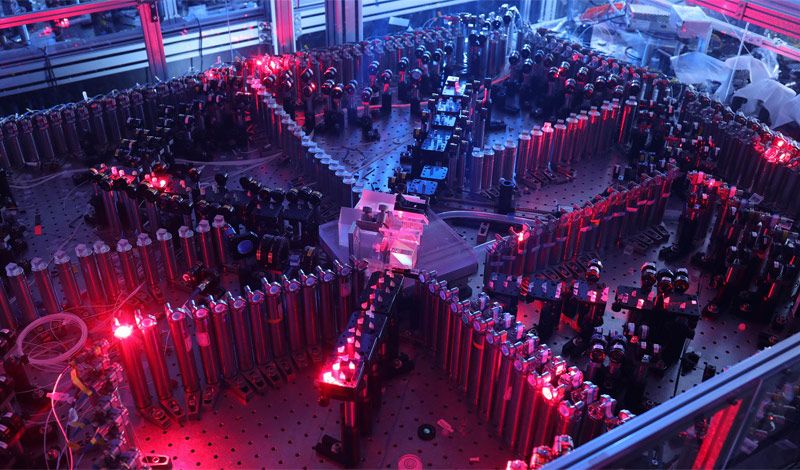

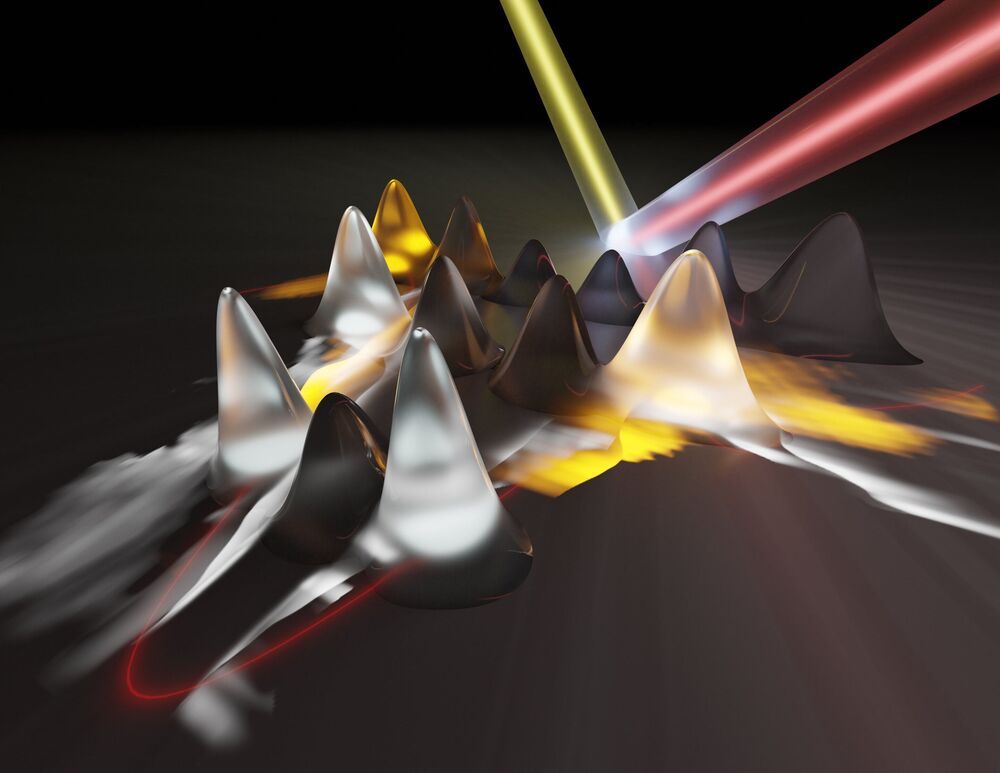
A new tool that uses light to map out the electronic structures of crystals could reveal the capabilities of emerging quantum materials and pave the way for advanced energy technologies and quantum computers, according to researchers at the University of Michigan, University of Regensburg and University of Marburg.
A paper on the work is published in Science.
Applications include LED lights, solar cells and artificial photosynthesis.
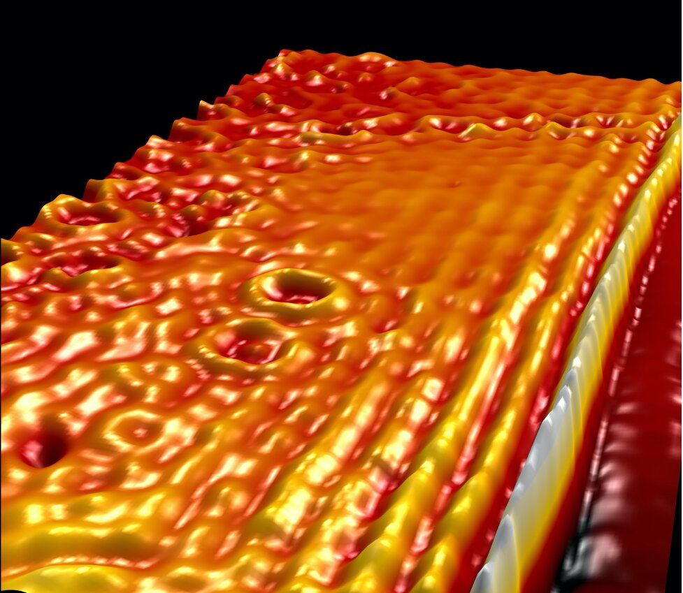
Graphene, an atomically thin carbon layer through which electrons can travel virtually unimpeded, has been extensively studied since its first successful isolation more than 15 years ago. Among its many unique properties is the ability to support highly confined electromagnetic waves coupled to oscillations of electronic charge—plasmon polaritons—that have potentially broad applications in nanotechnology, including biosensing, quantum information, and solar energy.
However, in order to support plasmon polaritons, graphene must be charged by applying a voltage to a nearby metal gate, which greatly increases the size and complexity of nanoscale devices. Columbia University researchers report that they have achieved plasmonically active graphene with record-high charge density without an external gate. They accomplished this by exploiting novel interlayer charge transfer with a two-dimensional electron-acceptor known as α-RuCl3. The study is available now online as an open access article and will appear in the December 9th issue of Nano Letters.
“This work allows us to use graphene as a plasmonic material without metal gates or voltage sources, making it possible to create stand-alone graphene plasmonic structures for the first time” said co-PI James Hone, Wang Fong-Jen Professor of Mechanical Engineering at Columbia Engineering.