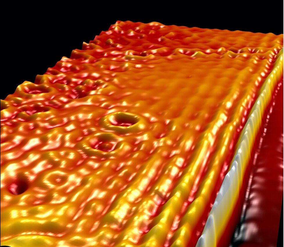
Graphene, an atomically thin carbon layer through which electrons can travel virtually unimpeded, has been extensively studied since its first successful isolation more than 15 years ago. Among its many unique properties is the ability to support highly confined electromagnetic waves coupled to oscillations of electronic charge—plasmon polaritons—that have potentially broad applications in nanotechnology, including biosensing, quantum information, and solar energy.
However, in order to support plasmon polaritons, graphene must be charged by applying a voltage to a nearby metal gate, which greatly increases the size and complexity of nanoscale devices. Columbia University researchers report that they have achieved plasmonically active graphene with record-high charge density without an external gate. They accomplished this by exploiting novel interlayer charge transfer with a two-dimensional electron-acceptor known as α-RuCl3. The study is available now online as an open access article and will appear in the December 9th issue of Nano Letters.
“This work allows us to use graphene as a plasmonic material without metal gates or voltage sources, making it possible to create stand-alone graphene plasmonic structures for the first time” said co-PI James Hone, Wang Fong-Jen Professor of Mechanical Engineering at Columbia Engineering.
