Toggle light / dark theme

A team of researchers from Heriot-Watt University, the Indian Institute of Technology and the University of Glasgow has demonstrated a way to transport entangled particles through a commercial fiber cable with 84.4% fidelity. In their paper published in the journal Nature Physics, the group describes using a unique attribute of entanglement to achieve such high fidelity. Andrew Forbes and Isaac Nape with the University of Witwatersrand have published a News & Views piece in the same journal issue outlining issues with sending entangled particles across fiber cables and the work done by the team in this new effort.

The study of entanglement, its properties and possible uses has made headlines due to its novelty and —particularly in quantum computers. One of the roadblocks standing in the way of its use as an international computer communications medium is noise encountered along the path through fiber cables that destroys the information they carry. In this new effort, the researchers have found a possible solution to the problem—using a unique attribute of entanglement to reduce losses due to noise.

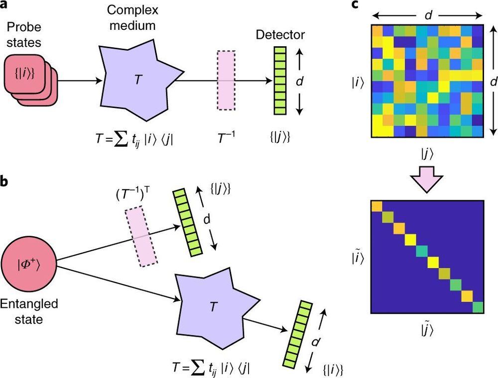
The work exploited a property of quantum physics that allows for mapping the medium (fiber cable) onto the quantum state of a particle moving through it. In essence, the entangled state of a particle (or photon in this context) created an image of the fiber cable, which allowed for reversing the scattering within it as a photon was transmitted. And furthermore, the descrambling could be achieved without having anything touch either the fiber or the photon that moved through it. More specifically, the researchers sent one of a pair of photons through a complex medium, but not the other. Both were then directed toward spatial light modulators and then on to detectors, and then finally to a device used to correlate coincidence counting. In their setup, light from the photon that did not pass through the complex medium propagated backward from the detector, allowing the photon to appear as if it had emerged from the crystal as the other photon.
A global research team has been able to transform brackish water and seawater into safe, clean drinking water in less than 30 minutes using metal-organic frameworks (MOFs) and sunlight.

In a discovery that could provide for millions of people across the world, researchers were not only able to filter harmful particles from and generate 139.5L of clean water per kilogram of MOF per day, but also perform this task in a more energy-efficient manner than current desalination practices.

The World Health Organization suggests good quality drinking water should have a total dissolved solid (TDS) of 600 parts per million (ppm). Researchers were able to achieve a TDS of 500 ppm in just 30 minutes and regenerate the MOF for reuse in four minutes under sunlight.

Most of the time, a material’s color stems from its chemical properties. Different atoms and molecules absorb different wavelengths of light; the remaining wavelengths are the “intrinsic colors” that we perceive when they are reflected back to our eyes.

So-called “” works differently; it’s a property of physics, not chemistry. Microscopic patterns on some surfaces reflect light in such a way that different wavelengths collide and interfere with one another. For example, a peacock’s feathers are made of transparent protein fibers that have no intrinsic color themselves, yet we see shifting, iridescent blue, green and purple hues because of the nanoscale structures on their surfaces.

As we become more adept at manipulating structure at the smallest scales, however, these two types of color can combine in even more surprising ways. Penn Engineers have now developed a system of nanoscale semiconductor strips that uses structural color interactions to eliminate the strips’ intrinsic color entirely.

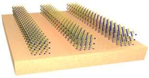
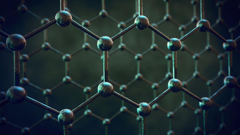
Scientists at the University of Bath have taken an important step towards understanding the interaction between layers of atomically thin materials arranged in stacks. They hope their research will speed up the discovery of new, artificial materials, leading to the design of electronic components that are far tinier and more efficient than anything known today.

Smaller is always better in the world of electronic circuitry, but there’s a limit to how far you can shrink a silicon component without it overheating and falling apart, and we’re close to reaching it. The researchers are investigating a group of atomically thin materials that can be assembled into stacks. The properties of any final material depend both on the choice of raw materials and on the angle at which one layer is arranged on top of another.

Dr. Marcin Mucha-Kruczynski who led the research from the Department of Physics, said: “We’ve found a way to determine how strongly atoms in different layers of a stack are coupled to each other, and we’ve demonstrated the application of our idea to a structure made of .”

The life-givers of integrated circuits and quantum devices in silicon are small structures made from patches of foreign atoms called dopants. The dopant structures provide charge carriers that flow through the components of the circuit, giving the components their ability to function. These days the dopant structures are only a few atoms across and so need to be made in precise locations within a circuit and have very well-defined electrical properties. At present manufacturers find it hard to tell in a non-destructive way whether they have made their devices according to these strict requirements. A new imaging paradigm promises to change all that.

The imaging mode called broadband electric force microscopy, developed by Dr. Georg Gramse at Keysight technologies & JKU uses a very sharp probe that sends into a silicon chip, to image and localize structures underneath the surface. Dr. Gramse says that because the microscope can use waves with many frequencies it can provide a wealth of previously inaccessible detail about the electrical environment around the dopant structures. The extra information is crucial to predicting how well the devices will ultimately perform.

The imaging approach was tested on two tiny dopant structures made with a templating process which is unique in achieving atomically sharp interfaces between differently doped regions. Dr. Tomas Skeren at IBM produced the world’s first electronic diode (a circuit component which passes current in only one direction) fabricated with this templating process, while Dr. Alex Kölker at UCL created a multilevel 3D with atomic scale precision.

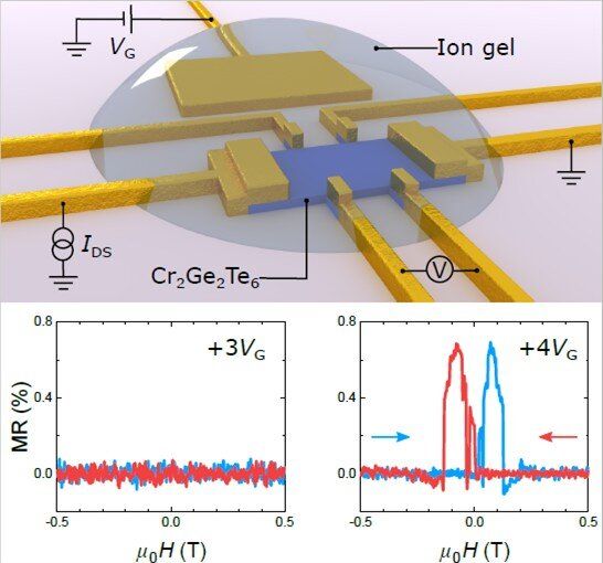
NUS physicists have demonstrated the control of magnetism in a magnetic semiconductor via electrical means, paving the way for novel spintronic devices.

Semiconductors are the heart of information-processing technologies. In the form of a transistor, semiconductors act as a switch for , allowing switching between binary states zero and one. Magnetic materials, on the other hand, are an essential component for information storage devices. They exploit the spin degree of freedom of electrons to achieve memory functions. Magnetic semiconductors are a unique class of materials that allow control of both the electrical charge and spin, potentially enabling information processing and memory operations in a single platform. The key challenge is to control the electron spins, or magnetisation, using electric fields, in a similar way a transistor controls electrical charge. However, magnetism typically has weak dependence on electric fields in magnetic semiconductors, and the effect is often limited to .

A research team led by Prof Goki EDA from the Department of Physics and the Department of Chemistry, and the Centre for Advanced 2-D Materials, NUS, in collaboration with Prof Hidekazu KUREBAYASHI from the London Centre for Nanotechnology, University College London, discovered that the magnetism of a magnetic semiconductor, Cr2Ge2Te6, shows exceptionally strong response to applied electric fields. With electric fields applied, the material was found to exhibit ferromagnetism (a state in which electron spins spontaneously align) at temperatures up to 200 K (−73°C). At such temperatures, ferromagnetic order is normally absent in this material.

O,.o well then anything could be a computer even a mushroom or a rock :3.


A complex process can modify non-magnetic oxide materials in such a way to make them magnetic. The basis for this new phenomenon is controlled layer-by-layer growth of each material. An international research team with researchers from Martin Luther University Halle-Wittenberg (MLU) reported on their unexpected findings in the journal Nature Communications.

In solid-state physics, oxide layers only a few nanometres thick are known to form a so-called two-dimensional electron gas. These thin layers, separated from one another, are transparent and electrically insulating materials. However, when one grows on top of the other, a conductive area forms under certain conditions at the interface, which has a metallic shine. “Normally this system remains non-magnetic,” says Professor Ingrid Mertig from the Institute of Physics at MLU. The research team has succeeded in controlling conditions during growth so that vacancies are created in the atomic layers near the interface. These are later filled in by other atoms from adjoining atomic layers.

The and explanations for this newly discovered phenomenon were made by Ingrid Mertig’s team of physicists. The method was then experimentally tested by several research groups throughout Europe—including a group led by Professor Kathrin Dörr from MLU. They were able to prove the magnetism in the materials. “This combination of computer simulations and experiments enabled us to decipher the complex mechanism responsible for the development of magnetism,” explains Mertig.