Toggle light / dark theme

In case you missed it, Elon Musk called BS on the field of nanotechnology last week. The ensuing Twitter spat was admittedly rather small on the grand scale of things.

But it did throw up an important question: just what is nanotech, and where does the BS end and the science begin?

I have a sneaky suspicion that Musk was trolling with his initial nano-comment. After all, much of the tech in his cars, solar cells and rockets relies on nanoscale science and engineering.

Read more

Glioblastoma is one of the most deadly forms of cancer. Affecting the brain, those unlucky enough to receive a diagnosis don’t have many treatment options – and usually a median life expectancy of just over a year. Now, researchers at MIT have developed nanoparticles that could provide hope, crossing the blood-brain barrier and delivering two types of drugs to fight tumors.

The MIT nanoparticles are liposomes, fatty droplets that can carry one drug on the inside and another in the outer layer. On the inside, the particles were loaded with a common chemotherapy drug called temozolomide, while the outer shell contained a more experimental substance known as JQ-1.

Read more

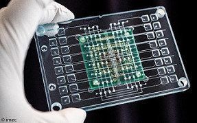
Imec, the world-leading research and innovation hub in nano-electronics and digital technologies, presents this week at its technology forum ITF 2018 (Antwerp, May 23–24), a novel organ-on-chip platform for pharmacological studies with unprecedented signal quality. It fuses imec’s high-density multi-electrode array (MEA)-chip with a microfluidic well plate, developed in collaboration with Micronit Microtechnologies, in which cells can be cultured, providing an environment that mimics human physiology. Capable of performing multiple tests in parallel, the new device aims to be a game-changer for the pharmaceutical industry, offering high quality data in the drug development process.

Every year a handful of new drugs make it to the market, but in their wake tens of thousands of candidate drugs didn’t make the cut. Nevertheless, this journey will have taken a decade and costs billions. The fact that is so time-consuming and costly, is because of the insufficiency of the existing methodologies for screening assays. These current assays are based on poor cell models that limit the quality of the resulting data, and result in inadequate biological relevance. Additionally, there is a lack of spatial resolution of the assays, resulting in the inability to screen single cells in a cell culture. Imec’s novel organ-on-chip platform aims to address these shortcomings and challenges.

Imec’s solution packs 16,384 electrodes, distributed over 16 wells, and offers multiparametric analysis. Each of the 1,024 electrodes in a well can detect intracellular action potentials, aside from the traditional extracellular signals. Further, ’s chip is patterned with microstructures to allow for a structured cell growth mimicking a specific organ.

Read more

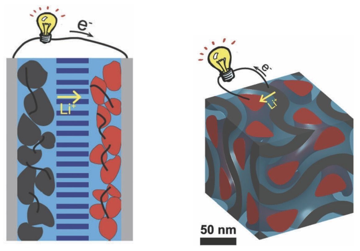
Left: Conventional composite battery design, with 2D stacked anode and cathode (black and red materials). Right: New 3D nanohybrid lithium-ion battery design, with multiple anodes and cathodes nanometers apart for high-speed charging. (credit: Cornell University)

Cornell University engineers have designed a revolutionary 3D lithium-ion battery that could be charged in just seconds.

In a conventional battery, the battery’s anode and cathode (the two sides of a battery connection) are stacked in separate columns (the black and red columns in the left illustration above). For the new design, the engineers instead used thousands of nanoscale (ultra-tiny) anodes and cathodes (shown in the illustration on the right above).

Read more

The world is a big place, but it’s gotten smaller with the advent of technologies that put people from across the globe in the palm of one’s hand. And as the world has shrunk, it has also demanded that things happen ever faster—including the time it takes to charge an electronic device.

A cross-campus collaboration led by Ulrich Wiesner, professor of engineering in the at Cornell University, addresses this demand with a novel architecture that has the potential for lightning-quick charges.

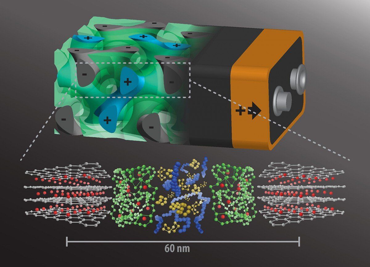
The group’s idea: Instead of having the batteries’ anode and cathode on either side of a nonconducting separator, intertwine the components in a self-assembling, 3D gyroidal structure, with thousands of nanoscale pores filled with the elements necessary for energy storage and delivery.

Read more

Q) Why Algorithmic leaps can be better than Hardware leaps?

Ans) Hardware constraints create bottlenecks that are hard to tackle as uncertainty of physics at small scale (nano-meters and less) come into play (electrons start jumping around).

At this point, ideas (algorithms) can be used to unleash full potential of the feasible hardware.

Read more

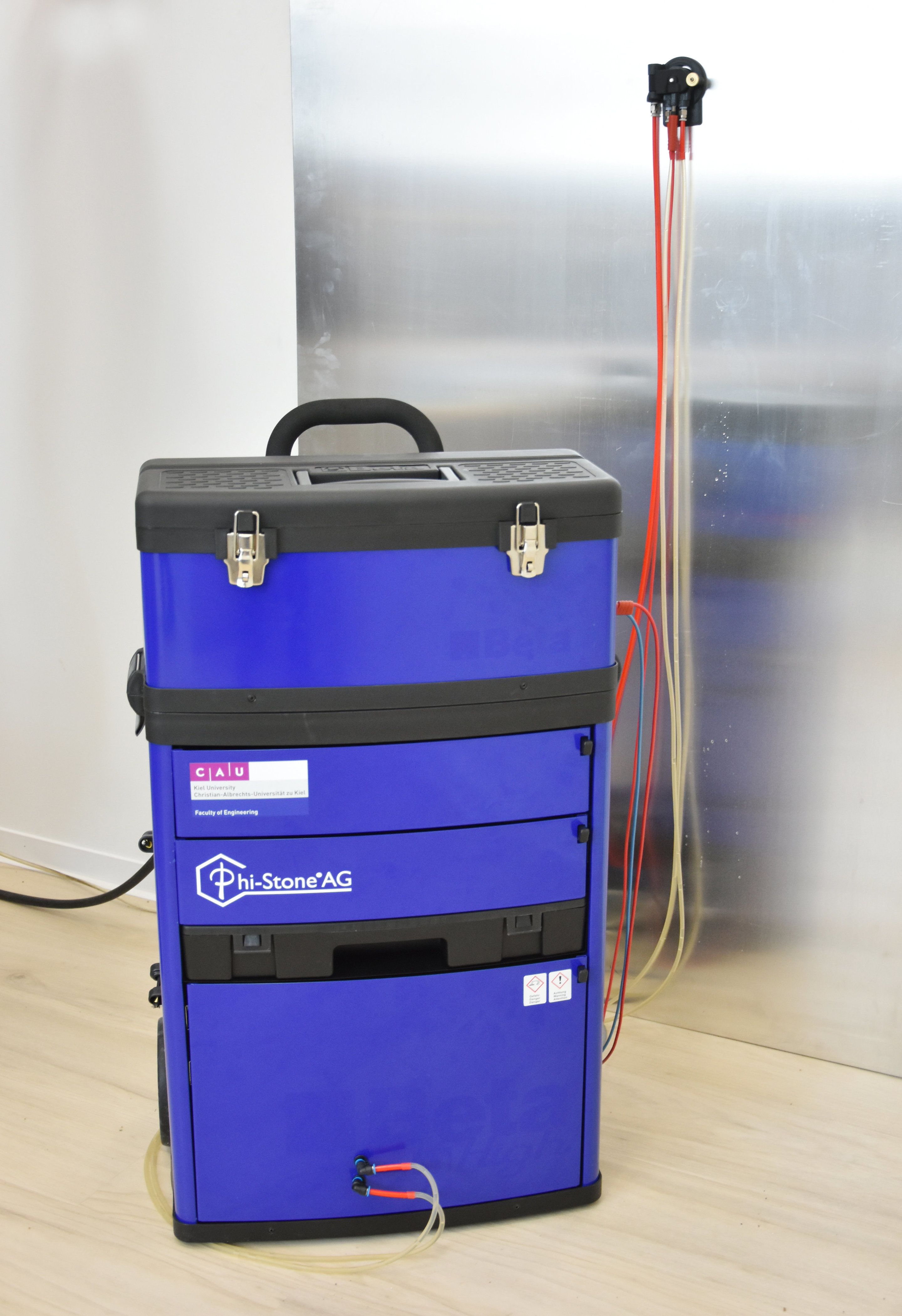
Welding is still the standard technique for joining metals. However, this laborious process carried out at high temperatures is not suitable for all applications. Now, a research team from the “Functional Nanomaterials” working group at Kiel University, together with the company Phi-Stone AG from Kiel, has developed a versatile alternative to conventional welding and gluing processes. Based on a special etching process, it enables aluminium and aluminium alloys to be joined with each other as well as with polymers, forming a durable and strong joint. They will present the prototype of a mobile joining unit at the Hannover Messe (23—27 April). They plan to commence mass production in future, after feedback from customers.

When welding, components are joined by locally melting them at the connection point. However, the required for this influence the material in the so-called heat-affected zone, causing structural as well as optical changes. It also requires special safety precautions and appropriately qualified staff. In contrast, the process developed by the Kiel University research group led by Professor Rainer Adelung not only spares the materials to be joined, but it is also easier and more flexible to use, even in hard-to-reach places such as corners or upside down on the ceiling. In just a few minutes, metals can be permanently connected with each other, but also with polymers.

The team envisages areas of application such as ship, aircraft or vehicle production. The process is particularly well-suited for subsequently attaching components in existing constructions, for example, in the interiors of ships or cars, explained Adelung regarding possible applications. “The high temperatures of welding will destroy surfaces that have already been treated and painted, for example. Our process, on the other hand, works at room temperature without special protective measures,” said Adelung.

Read more
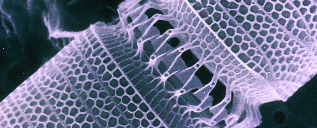
A new microchip technology capable of optically transferring data could solve a severe bottleneck in current devices by speeding data transfer and reducing energy consumption by orders of magnitude, according to an article published in the April 19, 2018 issue of Nature.

Researchers from Boston University, Massachusetts Institute of Technology, the University of California Berkeley and University of Colorado Boulder have developed a method to fabricate silicon chips that can communicate with light and are no more expensive than current technology. The result is the culmination of a several-year-long project funded by the Defense Advanced Research Project Agency that was a close collaboration between teams led by Associate Professor Vladimir Stojanovic of UC Berkeley, Professor Rajeev Ram of MIT, and Assistant Professor Milos Popovic from Boston University and previously CU Boulder. They collaborated with a semiconductor research team at the Colleges of Nanoscale Science and Engineering (CNSE) of the State University of New York at Albany.

The electrical signaling bottleneck between current microelectronic chips has left light communication as one of the only options left for further technological progress. The traditional method of data transfer-electrical wires-has a limit on how fast and how far it can transfer data. It also uses a lot of power and generates heat. With the relentless demand for higher performance and lower power in electronics, these limits have been reached. But with this new development, that bottleneck can be solved.

Read more

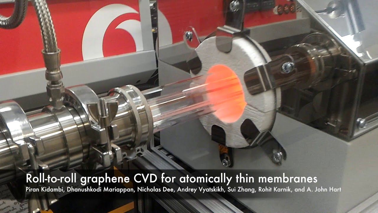
MIT engineers have developed a continuous manufacturing process that produces long strips of high-quality graphene.

The team’s results are the first demonstration of an industrial, scalable method for manufacturing high-quality that is tailored for use in membranes that filter a variety of molecules, including salts, larger ions, proteins, or nanoparticles. Such membranes should be useful for desalination, biological separation, and other applications.

“For several years, researchers have thought of graphene as a potential route to ultrathin membranes,” says John Hart, associate professor of mechanical engineering and director of the Laboratory for Manufacturing and Productivity at MIT. “We believe this is the first study that has tailored the manufacturing of graphene toward membrane applications, which require the graphene to be seamless, cover the substrate fully, and be of high quality.”

Read more

Human stem cells—the biological jack of all trades—have revolutionized modern medicine, with their ability to transform into specialized cell types.

But the current approach, which requires specialized instructive protein molecules known as growth factors, comes with risks, including the potential development of unwanted tissue, i.e., a tumor.

Researchers at Texas A&M University, however, have discovered a gentler approach.

Read more