Trash into treasure indeed. A European Union-funded research project is working on turning thrown-away food into graphene, the Guardian reports.
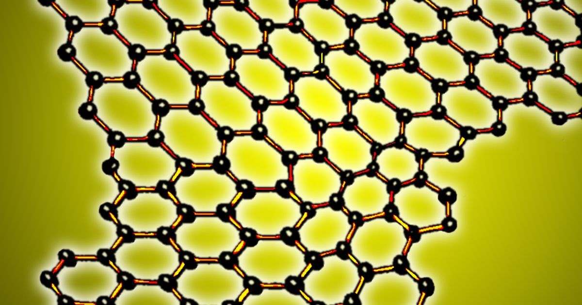

Trash into treasure indeed. A European Union-funded research project is working on turning thrown-away food into graphene, the Guardian reports.

A new type of energy storage system could revolutionise energy storage and drop the charging time of electric cars from hours to seconds.
In a new paper published today in the journal Nature Chemistry, chemists from the University of Glasgow discuss how they developed a flow battery system using a nano-molecule that can store electric power or hydrogen gas giving a new type of hybrid energy storage system that can be used as a flow battery or for hydrogen storage.
Their ‘hybrid-electric-hydrogen’ flow battery, based upon the design of a nanoscale battery molecule can store energy, releasing the power on demand as electric power or hydrogen gas that can be used a fuel. When a concentrated liquid containing the nano-molecules is made, the amount of energy it can store increases by almost 10 times. The energy can be released as either electricity or hydrogen gas meaning that the system could be used flexibly in situations that might need either a fuel or electric power.
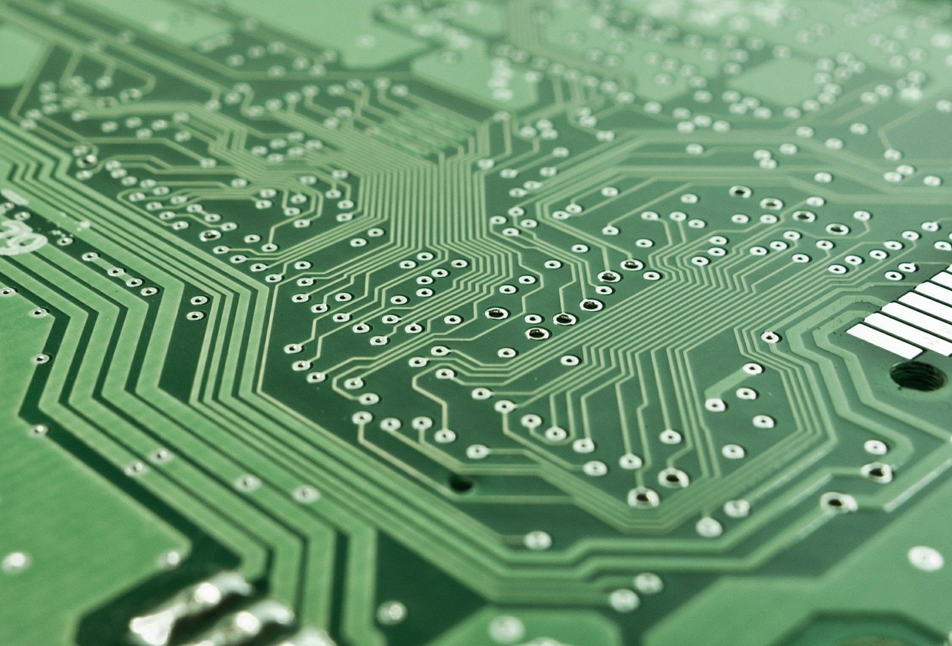
A new form of electronics manufacturing which embeds silicon nanowires into flexible surfaces could lead to radical new forms of bendable electronics, scientists say.
In a new paper published today in the journal Microsystems and Nanoengineering, engineers from the University of Glasgow describe how they have for the first time been able to affordably ‘print’ high-mobility semiconductor nanowires onto flexible surfaces to develop high-performance ultra-thin electronic layers.
Those surfaces, which can be bent, flexed and twisted, could lay the foundations for a wide range of applications including video screens, improved health monitoring devices, implantable devices and synthetic skin for prosthetics.
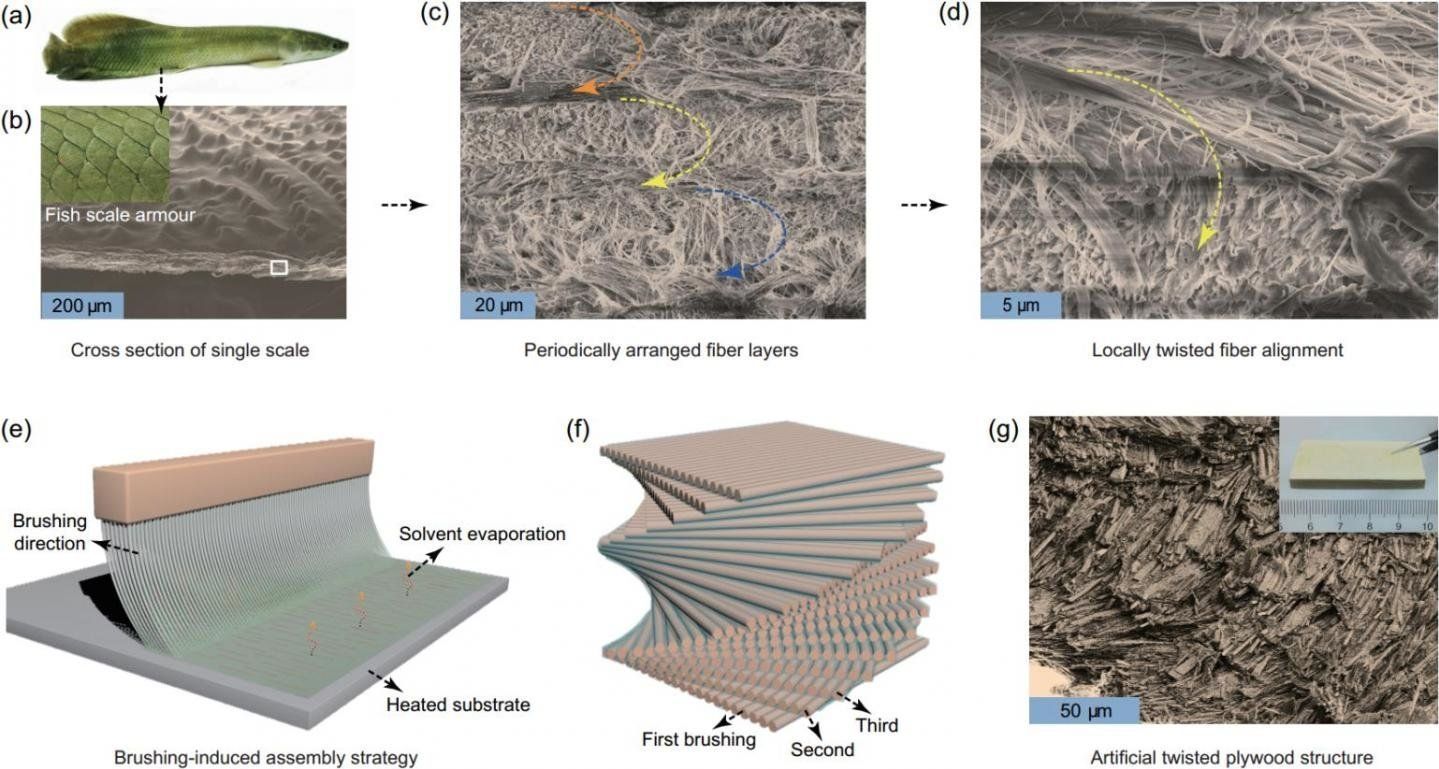
Over hundreds of millions of years of evolution, nature has produced a myriad of biological materials that serve either as skeletons or as defensive or offensive weapons. Although these natural structural materials are derived from relatively sterile natural components, such as fragile minerals and ductile biopolymers, they often exhibit extraordinary mechanical properties due to their highly ordered hierarchical structures and sophisticated interfacial design. Therefore, they are always a research subject for scientists aiming to create advanced artificial structural materials.
Through microstructural observation, researchers have determined that many biological materials, including fish scales, crab claws and bone, all have a characteristic “twisted plywood” structure that consists of a highly ordered arrangement of micro/nanoscale fiber lamellas. They are structurally sophisticated natural fiber-reinforced composites and often exhibit excellent damage tolerance that is desirable for engineering structural materials, but difficult to obtain. Therefore, researchers are seeking to mimic this kind of natural hierarchical structure and interfacial design by using artificial synthetic and abundant one-dimensional micro/nanoscale fibers as building blocks. In this way, they hope to produce high-performance artificial structural materials superior to existing materials.
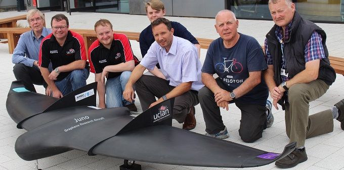
The University of Central Lancashire (UCLan) has unveiled the world’s first graphene skinned plane at an internationally renowned air show. Juno, a three-and-a-half-metre wide graphene skinned aircraft, was revealed on the North West Aerospace Alliance (NWAA) stand as part of the ‘Futures Day’ at Farnborough Air Show 2018.
The University’s aerospace engineering team has worked in partnership with the Sheffield Advanced Manufacturing Research Centre (AMRC), the University of Manchester’s National Graphene Institute (NGI), Haydale Graphene Industries (Haydale) and a range of other businesses to develop the unmanned aerial vehicle (UAV), which also includes graphene batteries and 3D printed parts.
Billy Beggs, UCLan’s Engineering Innovation Manager, said: The industry reaction to Juno at Farnborough was superb with many positive comments about the work we’re doing. Having Juno at one the world’s biggest air shows demonstrates the great strides we’re making in leading a programme to accelerate the uptake of graphene and other nano-materials into industry.
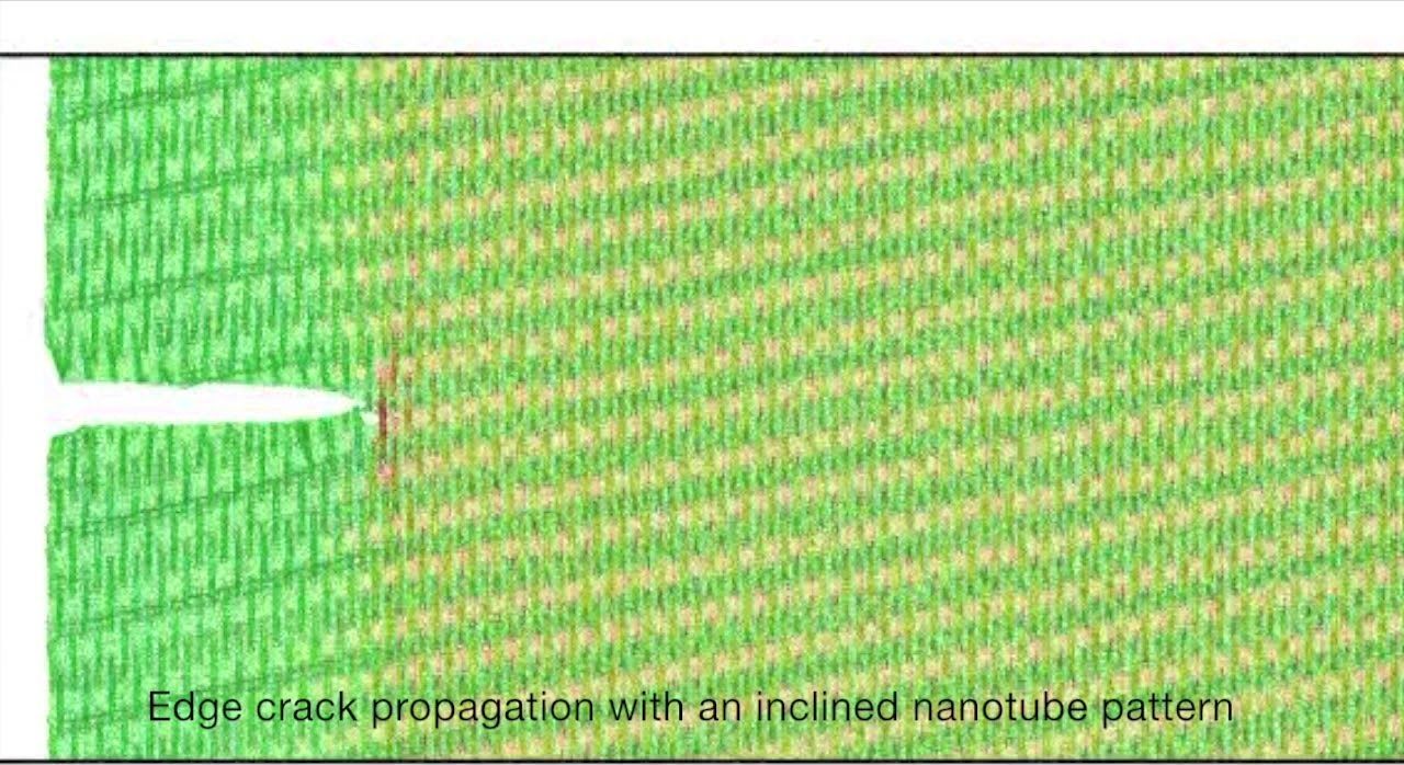
You may know graphene as a pseudo-legendary substance that could potentially revolutionize science and space travel and all sorts of things. If you don’t, you should get educated is pretty ridiculous. Simply made from carbon arranged into perfect one atom thing sheets makes the material one of the strongest ever observed. And, now, researchers at Rice University have found that so-called “rebar” graphene is dramatically tougher.
Graphene is much stronger than steel. In fact, an elephant could stand on a pencil and that pressure couldn’t break through a thin sheet of the material. But, because it is arranged in sheets, it can still be ripped if damaged from the right angle. But the researchers figured that reinforcing the structure, as we do with steel bars in concrete structures, l could help prevent damage.
The new research, published in the ACS Nano, a journal run by the American Chemical Society, Rice materials scientist Jun Lou and lead author Emily Hacopian examined the properties of rebar graphene under stress. Cracked and tears in the structure that otherwise would have spread across the sheet are stopped by the reinforcement while also staying stretchy and pliable.
Closing in on molecular manufacturing…
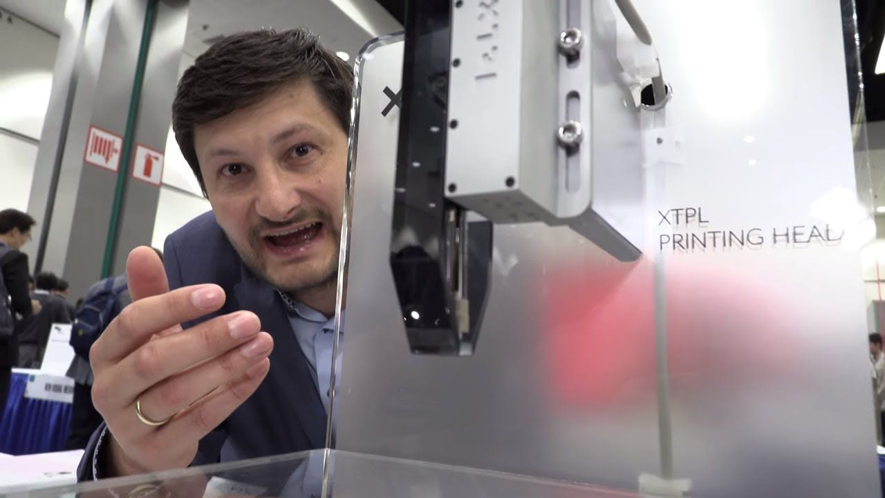
http://xt-pl.com received an honorable mention from I-Zone judges for its innovative product that prints extremely fine film structures using nanomaterials. XTPL’s interdisciplinary team is developing and commercializing an innovative technology that enables ultra-precise printing of electrodes up to several hundred times thinner than a human hair – conducive lines as thin as 100 nm. XTPL is facilitating the production of a new generation of transparent conductive films (TCFs) that are widely used in manufacturing. XTPL’s solution has a potentially disruptive technology in the production of displays, monitors, touchscreens, printed electronics, wearable electronics, smart packaging, automotive, medical devices, photovoltaic cells, biosensors, and anti-counterfeiting. The technology is also applicable to the open-defect repair industry (the repair of broken metallic connections in thin film electronic circuits) and offers cost-effective, non-toxic, flexible industry-adapted solutions.
XTPL’s technology might be the only one in the world offering cost-effective, non-toxic, flexible, industry adapted solution for the market of displays TFT/LCD/OLED, integrated circuits (IC), printed circuit boards (PCB), multichip modules (MCM); photolithographic masks & solar cells market.
XTPL delivers also solutions for research & prototyping including printing head, electronics, software algorithms which are the core of the system driving the electric field and the assembly process of nanoparticles implemented in XTPL’s Nanometric Lab Printer. It is a device that offers necessary functionalities to test, evaluate and use XTPL line-forming technology with nanometric precision and enables positioning of the printing head with micrometric resolution precisely.
Official video explaining XTPL’s technology: https://youtu.be/WMerzxzCXuw
Filmed at the I-Zone demo and prototype area at SID Display Week, the world’s largest and best exhibition for electronic information display technology.

The trouble with microphones is that they don’t just hear — they have to listen. Powering the mic and its signal processor means using energy, and energy means a battery, and a battery means charging. This new microphone-like system hears more like the way our own ears do, requiring little or no power, and could help fill the world with voice-responsive machines. (If that’s something we really want.)
The device is called a “triboelectric auditory sensor,” and it works via what’s called the triboelectric effect — essentially when two surfaces rub together and create a charge. They’re still trying to figure out why this happens, but what matters to engineers is that it happens reliably.
Triboelectric nanogenerators have been around for a few years, creating power by having two compatible materials interact with each other at super-small scales. While they’re tiny and highly efficient, they don’t actually produce a lot of power. Researchers from Chongqing University found that, fortunately, you don’t need a lot of power for the purposes of detecting sound.

Robots like this, nanobots that can work in the body, should be the main focus for curing all disease. And instead of focusing on Drug Delivery, have the nanobots just go in and attack or fix the problem themselves.
A Brock University research team has created a microscopic robot that has the potential to identify drug resistance to tuberculosis faster than conventional tests.
The World Health Organization (WHO) calls tuberculosis drug resistance “a formidable obstacle” to treatment and prevention of a disease that killed 240,000 people in 2016.
The Brock team’s latest technology builds on an earlier version of the microscopic robot—called the three-dimensional DNA nanomachine—they created in 2016 to detect diseases in a blood sample within 30 minutes.
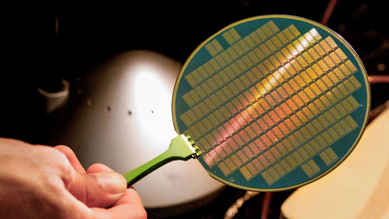
Silicon computer chips have been on a roll for half a century, getting ever more powerful. But the pace of innovation is slowing. Today the U.S. military’s Defense Advanced Research Projects Agency (DARPA) announced dozens of new grants totaling $75 million in a program that aims to reinvigorate the chip industry with basic research into new designs and materials, such as carbon nanotubes. Over the next few years, the DARPA program, which supports both academic and industry scientists, will grow to $300 million per year up to a total of $1.5 billion over 5 years.
“It’s a critical time to do this,” says Erica Fuchs, a computer science policy expert at Carnegie Mellon University in Pittsburgh, Pennsylvania.
In 1965, Intel co-founder Gordon Moore made the observation that would become his eponymous “law”: The number of transistors on chips was doubling every 2 years, a time frame later cut to every 18 months. But the gains from miniaturizing the chips are dwindling. Today, chip speeds are stuck in place, and each new generation of chips brings only a 30% improvement in energy efficiency, says Max Shulaker, an electrical engineer at the Massachusetts Institute of Technology in Cambridge. Fabricators are approaching physical limits of silicon, says Gregory Wright, a wireless communications expert at Nokia Bell Labs in Holmdel, New Jersey. Electrons are confined to patches of silicon just 100 atoms wide, he says, forcing complex designs that prevent electrons from leaking out and causing errors. “We’re running out of room,” he says.