Toggle light / dark theme

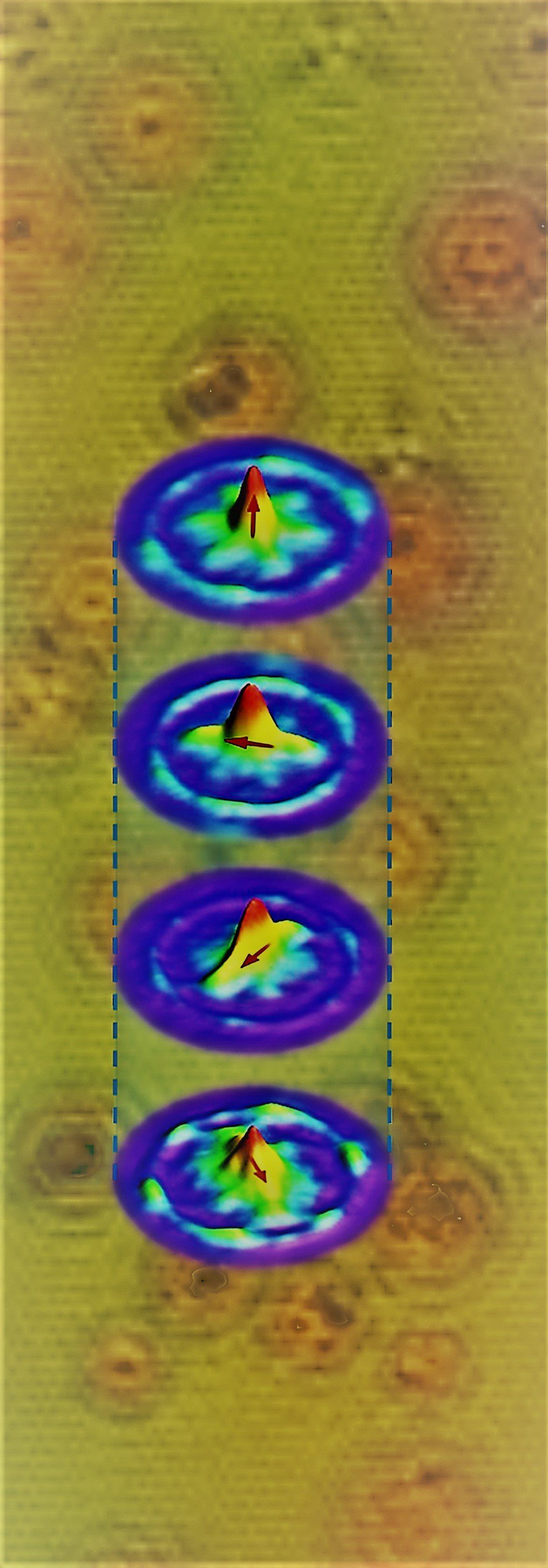
Quantum particles can be difficult to characterize, and almost impossible to control if they strongly interact with each other—until now.

An international team of researchers led by Princeton physicist Zahid Hasan has discovered a state of matter that can be “tuned” at will—and it’s 10 times more tuneable than existing theories can explain. This level of manipulability opens enormous possibilities for next-generation nanotechnologies and quantum computing.

“We found a new control knob for the quantum topological world,” said Hasan, the Eugene Higgins Professor of Physics. “We expect this is tip of the iceberg. There will be a new subfield of materials or physics grown out of this. … This would be a fantastic playground for nanoscale engineering.”
Read more

A recent discovery by William & Mary and University of Michigan researchers transforms our understanding of one of the most important laws of modern physics. The discovery, published in the journal Nature, has broad implications for science, impacting everything from nanotechnology to our understanding of the solar system.

“This changes everything, even our ideas about planetary formation,” said Mumtaz Qazilbash, associate professor of physics at William & Mary and co-author on the paper. “The full extent of what this means is an important question and, frankly, one I will be continuing to think about.”

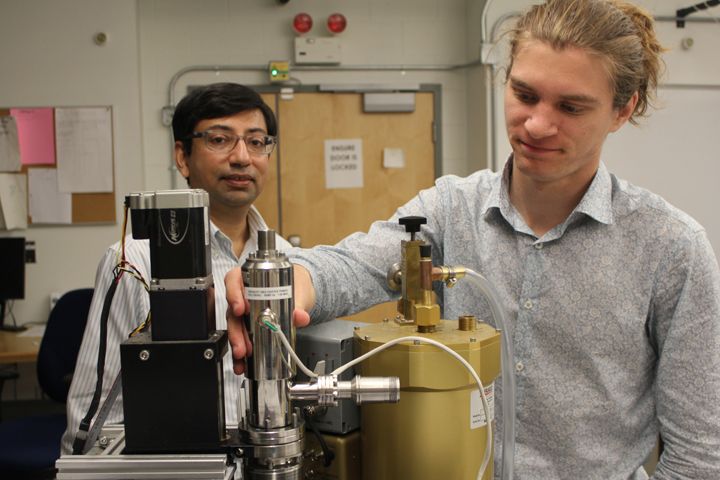
Qazilbash and two W&M graduate students, Zhen Xing and Patrick McArdle, were asked by a team of engineers from the University of Michigan to help them test whether Planck’s radiation law, a foundational scientific principle grounded in quantum mechanics, applies at the smallest length scales.

Read more

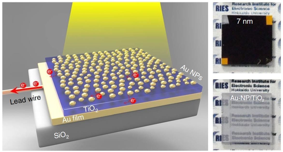
Scientists have developed a photoelectrode that can harvest 85 percent of visible light in a 30 nanometers-thin semiconductor layer between gold layers, converting light energy 11 times more efficiently than previous methods.

In the pursuit of realizing a sustainable society, there is an ever-increasing demand to develop revolutionary solar cells or artificial photosynthesis systems that utilize energy from the sun while using as few materials as possible.

The research team, led by Professor Hiroaki Misawa of the Research Institute for Electronic Science at Hokkaido University, has been aiming to develop a photoelectrode that can harvest visible light across a wide spectral range by using loaded on a semiconductor. But merely applying a layer of gold nanoparticles did not lead to a sufficient amount of , because they took in light with only a narrow spectral range.

Read more

A 2011 invention made by Aalto University’s researchers has proceeded from concept to reality. Just a few years ago the researchers obtained the record efficiency of 22% in the lab for nanostructured solar cells using atomic layer deposition, and now with the help of industrial partners and joint European collaboration, the first prototype modules have been manufactured on an industrial production line.

“Our timing could not have been better” prof. Hele Savin, who led the research, was pleased to tell. Indeed, 2018 is commonly called the “Year of Black Silicon” due to its rapid expansion in the photovoltaic (PV) industry. It has enabled the use of diamond-wire sawing in multicrystalline silicon, which reduces costs and environmental impact. However, there is still plenty of room for improvement as the current used in industry consists of shallow nanostructures that leads to sub-optimal optical properties and requires a separate antireflection coating.

Aalto’s approach consists of using deep needle-like nanostructures to make an optically perfect surface that eliminates the need for the antireflection coatings. Their industrial production, however, was not an easy task. “We were worried that such a fragile structure would not survive the multi-step mass production, because of rough handling by robots or module lamination.”

Read more

Rice University atomic physicists have verified a key prediction from a 55-year-old theory about one-dimensional electronics that is increasingly relevant thanks to Silicon Valley’s inexorable quest for miniaturization.

“Chipmakers have been shrinking feature sizes on microchips for decades, and device physicists are now exploring the use of nanowires and nanotubes where the channels that electrons pass through are almost one-dimensional,” said Rice experimental physicist Randy Hulet. “That’s important because 1D is a different ballgame in terms of electron conductance. You need a new model, a new way of representing reality, to make sense of it.”

With IBM and others committed to incorporating one-dimensional carbon nanotubes into integrated circuits, chip designs will increasingly need to account for 1D effects that arise from electrons being fermions, antisocial particles that are unwilling to share space.

Read more

In 2018, Canada is ranked tenth in the world in nominal GDP. It is a rich developed country. Despite having an economy that is 11 times smaller than the USA or 7 times smaller than China, Canada has world competitive or world-leading projects in quantum computing, artificial intelligence, molecular nanotechnology, nuclear fusion and nuclear-molten salt.

Read more