Author at The Secrets of the Universe, I am a Biology and Chemistry high school student from Poland. I love writing about conquest and research in space and future possibilities for Humanity and Astrophysics.


Author at The Secrets of the Universe, I am a Biology and Chemistry high school student from Poland. I love writing about conquest and research in space and future possibilities for Humanity and Astrophysics.

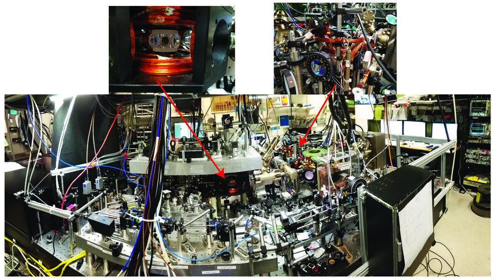
The concept of universal physics is intriguing, as it enables researchers to relate physical phenomena in a variety of systems, irrespective of their varying characteristics and complexities. Ultracold atomic systems are often perceived as ideal platforms for exploring universal physics, owing to the precise control of experimental parameters (such as the interaction strength, temperature, density, quantum states, dimensionality, and the trapping potential) that might be harder to tune in more conventional systems. In fact, ultracold atomic systems have been used to better understand a myriad of complex physical behavior, including those topics in cosmology, particle, nuclear, molecular physics, and most notably, in condensed matter physics, where the complexities of many-body quantum phenomena are more difficult to investigate using more traditional approaches.
Understanding the applicability and the robustness of universal physics is thus of great interest. Researchers at the National Institute of Standards and Technology (NIST) and the University of Colorado Boulder have carried out a study, recently featured in Physical Review Letters, aimed at testing the limits to universality in an ultracold system.
“Unlike in other physical systems, the beauty of ultracold systems is that at times we are able to scrap the importance of the periodic table and demonstrate the similar phenomenon with any chosen atomic species (be it potassium, rubidium, lithium, strontium, etc.),” Roman Chapurin, one of the researchers who carried out the study, told Phys.org. “Universal behavior is independent of the microscopic details. Understanding the limitations of universal phenomenon is of great interest.”
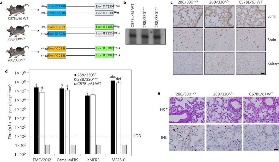
A, C57BL/6J mice were genetically engineered using CRISPR–Cas9 genomic editing to encode 288L and 330R in mDPP4 on one chromosome (heterozygous, 288/330+/−) or on both chromosomes (homozygous, 288/330+/+). b, Northern blot of mDPP4 mRNA expression. c, Immunohistochemistry (IHC) of mDPP4 protein in the lungs, brain and kidneys of individual C57BL/6J wild-type (WT), 288/330+/− and 288/330+/+ mice. d, Viral titres for MERS-CoV at 3 days post-infection from C57BL/6J WT, 288/330+/− and 288/330+/+ (all n = 4) mice infected with 5 × 10⁵ plaque-forming units (p.f.u.) of the indicated viruses. Bar graphs show means + s.d.
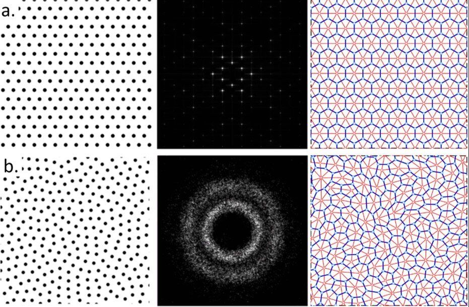
In a new report published on Scientific Reports, Milan M. Milošević and an international research team at the Zepler Institute for Photonics and Nanoelectronics, Etaphase Incorporated and the Departments of Chemistry, Physics and Astronomy, in the U.S. and the U.K. Introduced a hyperuniform-disordered platform to realize near-infrared (NIR) photonic devices to create, detect and manipulate light. They built the device on a silicon-on-insulator (SOI) platform to demonstrate the functionality of the structures in a flexible, silicon-integrated circuit unconstrained by crystalline symmetries. The scientists reported results for passive device elements, including waveguides and resonators seamlessly integrated with conventional silicon-on-insulator strip waveguides and vertical couplers. The hyperuniform-disordered platform improved compactness and enhanced energy efficiency as well as temperature stability, compared to silicon photonic devices fabricated on rib and strip waveguides.
Academic and commercial efforts worldwide in the field of silicon photonics have led to engineer optical data communications at the Terabit-scale at increasingly lower costs to meet the rapidly growing demand in data centers. Explosive growth in cloud computing and entertainment-on-demand pose increasingly challenging costs and energy requirements for data transmission, processing and storage. Optical interconnects can replace traditional copper-based solutions to offer steadily increasing potential to minimize latency and power consumption, while maximizing the bandwidth and reliability of the devices. Silicon photonics also leverage large-scale, complementary metal-oxide semiconductor (CMOS) manufacturing processes to produce high-performance optical transceivers with high yield at low-cost. The properties allow applications of optical transceivers (fiber optical technology to send and receive data) to be increasingly compelling across shorter distances.
More than three decades ago, physicist Richard Soref identified silicon as a promising material for photonic integration. Leading to the present-day steady development and rapid production of increasingly complex photonic integrated circuits (PICs). Researchers can integrate large numbers of massively-parallel compact energy-efficient optical components on a single chip for cloud computing applications from deep learning to artificial intelligence and the internet of things. Compared to the limited scope of commercial silicon photonic systems, photonic crystal (PhC) architectures promise smaller device sizes, although they are withheld by layout constraints imposed by waveguide requirements along the photonic crystal’s axis. Until recently, photonic band gap (PBG) structures that efficiently guide light were limited to photonic crystal platforms. Now, newer classes of PBG structures include photonic quasicrystals, hyperuniform disordered solids (HUDs) and local self-uniform structures.
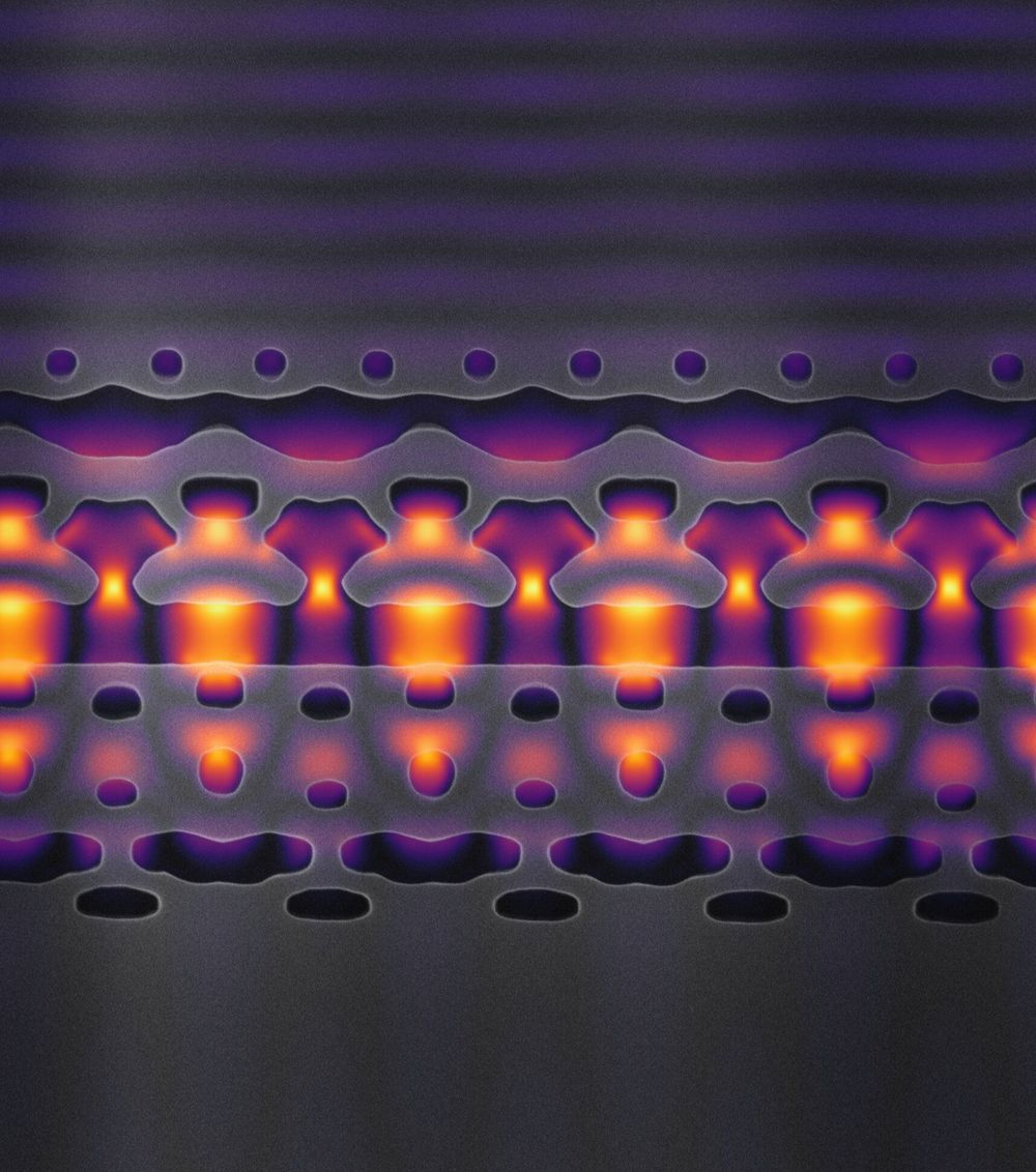
The accelerator-on-a-chip demonstrated in Science is just a prototype, but Vuckovic said its design and fabrication techniques can be scaled up to deliver particle beams accelerated enough to perform cutting-edge experiments in chemistry, materials science and biological discovery that don’t require the power of a massive accelerator.
“The largest accelerators are like powerful telescopes. There are only a few in the world and scientists must come to places like SLAC to use them,” Vuckovic said. “We want to miniaturize accelerator technology in a way that makes it a more accessible research tool.”
Team members liken their approach to the way that computing evolved from the mainframe to the smaller but still useful PC. Accelerator-on-a-chip technology could also lead to new cancer radiation therapies, said physicist Robert Byer, a co-author of the Science paper. Again, it’s a matter of size.
Today, medical X-ray machines fill a room and deliver a beam of radiation that’s tough to focus on tumors, requiring patients to wear lead shields to minimize collateral damage.
On a hillside above Stanford University, the SLAC National Accelerator Laboratory operates a scientific instrument nearly 2 miles long. In this giant accelerator, a stream of electrons flows through a vacuum pipe, as bursts of microwave radiation nudge the particles ever-faster forward until their velocity approaches the speed of light, creating a powerful beam that scientists from around the world use to probe the atomic and molecular structures of inorganic and biological materials.
Now, for the first time, scientists at Stanford and SLAC have created a silicon chip that can accelerate electrons—albeit at a fraction of the velocity of that massive instrument—using an infrared laser to deliver, in less than a hair’s width, the sort of energy boost that takes microwaves many feet.
Writing in the Jan. 3 issue of Science, a team led by electrical engineer Jelena Vuckovic explained how they carved a nanoscale channel out of silicon, sealed it in a vacuum and sent electrons through this cavity while pulses of infrared light—to which silicon is as transparent as glass is to visible light—were transmitted by the channel walls to speed the electrons along.
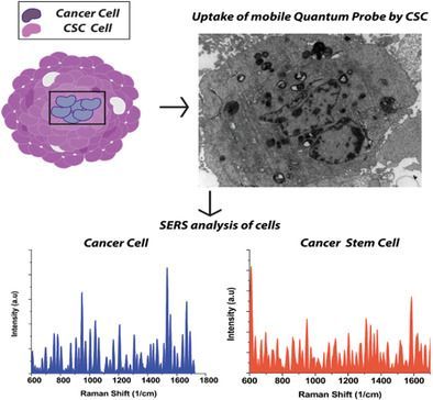
Cancer stem cells (CSC) are believed to be the driving force of cancer metastases and are a rare population of self‐renewing cells that contribute majorly to the poor outcomes of cancer therapy. The detection of CSC is of utmost importance to shed light on the indestructible nature of certain solid tumors and their metastatic ability. However, tumors tend to harbor CSCs in a specialized niche, making the detection process difficult. Currently, there is no method available to detect CSCs. The significance of this work is twofold. First, to the best of the knowledge, it is the first time that the detection of CSC is demonstrated. This approach simultaneously detects both the phenotypic and the metabolic state of the cell, thus enabling universal detection of CSC with high accuracy. Second, to the best of the knowledge, for the first time, light is shed on cell chemistry of CSC in their dedicated niche to facilitate a better understanding of the key players involved in the metabolic rewiring of CSC. This work will enable a better understanding of the fundamentals of CSCs, which are critical for the early diagnosis of cancer and the development of therapies for the cure of cancer.

From insilico meddicine — the beginning of an AI healthcare revolution.
Poly Mamoshina on Machine Learning for small molecule drug discovery and the beginning of an AI healthcare revolution — interviewed at the Undoing Aging conference in Berlin 2019!
Polina Mamoshina is a senior research scientist at Insilico Medicine, Inc (www.insilico.com), a Baltimore-based bioinformatics and deep learning company focused on reinventing drug discovery and biomarker development and a part of the computational biology team of Oxford University Computer Science Department. Polina graduated from the Department of Genetics of the Moscow State University. She was one of the winners of GeneHack a Russian nationwide 48-hour hackathon on bioinformatics at the Moscow Institute of Physics and Technology attended by hundreds of young bioinformaticians. Polina is involved in multiple deep learning projects at the Pharmaceutical Artificial Intelligence division of Insilico Medicine working on the drug discovery engine and developing biochemistry, transcriptome, and cell-free nucleic acid-based biomarkers of aging and disease. She recently co-authored seven academic papers in peer-reviewed journals.
https://scholar.google.com/citations?user=YrLgl8gAAAAJ&hl=en
https://uk.linkedin.com/in/polymamoshina
https://cogx.co/speakers/polina-mamoshina/
Many thanks for watching!
Consider supporting SciFuture by:
a) Subscribing to the SciFuture YouTube channel: http://youtube.com/subscription_center?add_user=TheRationalFuture
b) Donating
- Bitcoin: 1BxusYmpynJsH4i8681aBuw9ZTxbKoUi22
- Etherium: 0xd46a6e88c4fe179d04464caf42626d0c9cab1c6b
- Patreon: https://www.patreon.com/scifuture
c) Sharing the media SciFuture creates: http://scifuture.org
Kind regards.
Adam Ford
- Science, Technology & the Future.
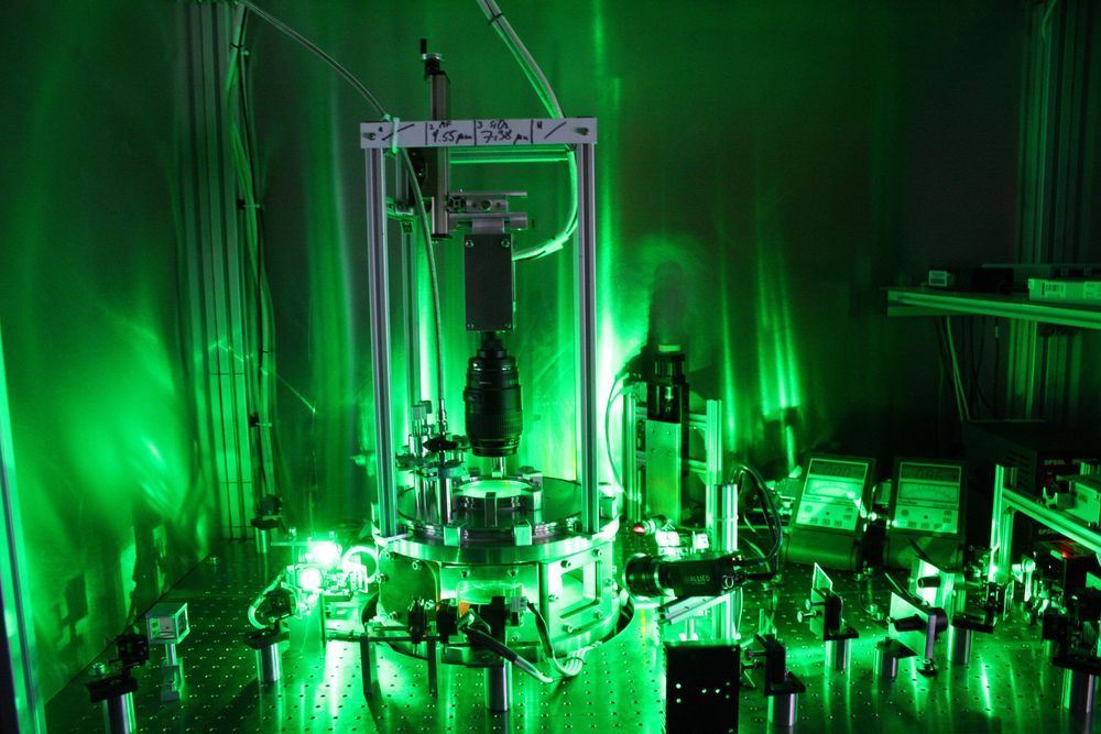
Since the end of the 19th century, physicists have known that the transfer of energy from one body to another is associated with entropy. It quickly became clear that this quantity is of fundamental importance, and so began its triumphant rise as a useful theoretical quantity in physics, chemistry and engineering. However, it is often very difficult to measure. Professor Dietmar Block and Frank Wieben of Kiel University (CAU) have now succeeded in measuring entropy in complex plasmas, as they reported recently in the renowned scientific journal Physical Review Letters. In a system of charged microparticles within this ionized gas, the researchers were able to measure all positions and velocities of the particles simultaneously. In this way, they were able to determine the entropy, as it was already described theoretically by the physicist Ludwig Boltzmann around 1880.
Surprising thermodynamic equilibrium in plasma
“With our experiments, we were able to prove that in the important model system of complex plasma, the thermodynamic fundamentals are fulfilled. What is surprising is that this applies to microparticles in a plasma, which is far away from thermodynamic equilibrium,” explains Ph.D. student Frank Wieben. In his experiments, he is able to adjust the thermal motion of the microparticles by means of a laser beam. Using video microscopy, he can observe the dynamic behaviour of the particles in real time, and determine the entropy from the information collected.
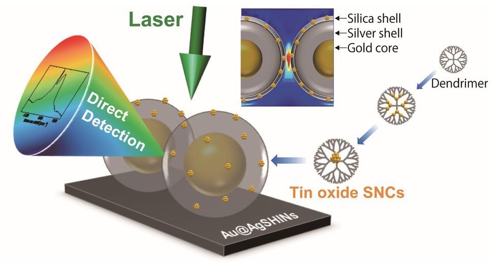
Scientists at Tokyo Institute of Technology (Tokyo Tech) have developed a new methodology that allows researchers to assess the chemical composition and structure of metallic particles with a diameter of only 0.5 to 2 nm. This breakthrough in analytical techniques will enable the development and application of minuscule materials in the fields of electronics, biomedicine, chemistry, and more.
The study and development of novel materials have enabled countless technological breakthroughs and are essential across most fields of science, from medicine and bioengineering to cutting-edge electronics. The rational design and analysis of innovative materials at nanoscopic scales allows us to push through the limits of previous devices and methodologies to reach unprecedented levels of efficiency and new capabilities. Such is the case for metal nanoparticles, which are currently in the spotlight of modern research because of their myriad potential applications. A recently developed synthesis method using dendrimer molecules as a template allows researchers to create metallic nanocrystals with diameters of 0.5 to 2 nm (billionths of a meter).