Toggle light / dark theme

Google is to trying to combine the Adiabatic Quantum computing AQC method with the digital approach’s error-correction capabilities.

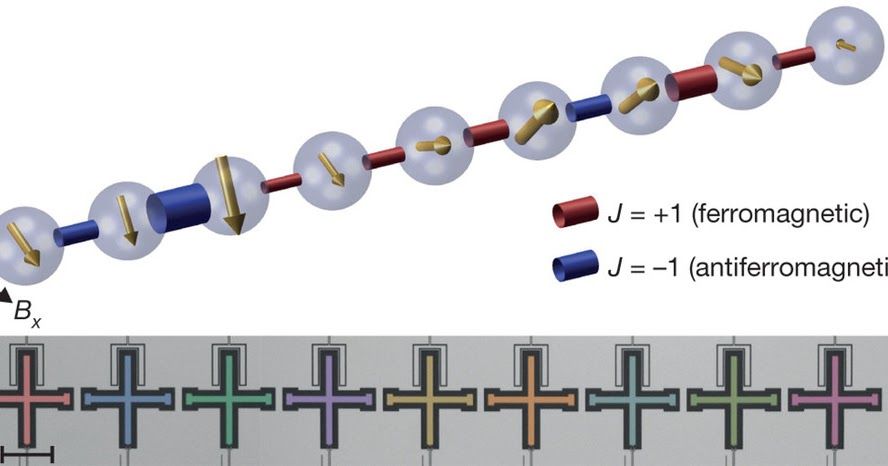
The Google team uses a row of nine solid-state qubits, fashioned from cross-shaped films of aluminium about 400 micrometres from tip to tip. These are deposited onto a sapphire surface. The researchers cool the aluminium to 0.02 degrees kelvin, turning the metal into a superconductor with no electrical resistance. Information can then be encoded into the qubits in their superconducting state.

The interactions between neighboring qubits are controlled by ‘logic gates’ that steer the qubits digitally into a state that encodes the solution to a problem. As a demonstration, the researchers instructed their array to simulate a row of magnetic atoms with coupled spin states — a problem thoroughly explored in condensed-matter physics. They could then look at the qubits to determine the lowest-energy collective state of the spins that the atoms represented.

Read more

Featuring backside-illuminated sensor technology providing 95% quantum efficiency, the Prime 95B from 2016 Innovators Awards silver-level honoree Photometrics is reportedly three times more sensitive than the current generation of sCMOS cameras. The camera features a GSENSE400BSI-TVISB scientific CMOS (sCMOS) sensor from Gpixel Inc., which is a 1.44 MPixel sensor with a 11 µm square pixel size that can achieve a frame rate of 41 fps in 16-bit and 82 fps in 12-bit. The Prime 95B, according to Photometrics, is optimized for low-light microscopy and life sciences imaging applications because of its ability to collect nearly all available light, and maximize the signal-to-noise ratio of the experiment while minimizing cellular photo damage. Additionally, the camera features forced air or liquid cooling options, as well as a PCIe and USB 3.0 interfaces.

Read more

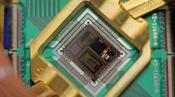
The QUTIS research group (www.qutisgroup.com) of the University of the Basque Country (UPV/EHU) and Google’s quantum computation team have collaborated on a pioneering experiment that universally digitizes analogue quantum computation on a superconducting chip. This breakthrough was made at Google’s labs in Santa Barbara (California) and has been published in the prestigious journal Nature.

Read more

Nice!


Scientists can now identify the exact location of a single atom in a silicon crystal, a discovery that is key for greater accuracy in tomorrow’s silicon based quantum computers.

It’s now possible to track and see individual phosphorus atoms in a silicon crystal allowing confirmation of quantum computing capability, but which also has use in nano detection devices.

Quantum computing has the potential for enormous processing power in the future. Current laptops have transistors that use a binary code, an on-or-off state (bits). But tomorrow’s quantum computers will use quantum bits ‘qubits’, which have multiple states.

Read more

Very promising. I imagine 3D Printers being able to create synthesize diamonds will be a very profitable business to get in to because of the stabilizing benefits that the nanodiamonds bring to Quantum Computing and nanotechnology in general.


Nanomaterials have the potential to improve many next-generation technologies. They promise to speed up computer chips, increase the resolution of medical imaging devices and make electronics more energy efficient. But imbuing nanomaterials with the right properties can be time consuming and costly. A new, quick and inexpensive method for constructing diamond-based hybrid nanomaterials could soon launch the field forward.

University of Maryland researchers developed a method to build diamond-based hybrid nanoparticles in large quantities from the ground up, thereby circumventing many of the problems with current methods. The technique is described in the June 8, 2016 issue of the journal Nature Communications (“Nanostructures for Coupling Nitrogen-Vacancy Centers to Metal Nanoparticles and Semiconductor Quantum Dots”).

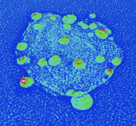
electron microscope image shows a hybrid nanoparticle consisting of a nanodiamond (roughly 50 nanometers wide) covered in smaller silver nanoparticles

This electron microscope image shows a hybrid nanoparticle consisting of a nanodiamond (roughly 50 nanometers wide) covered in smaller silver nanoparticles that enhance the diamond’s optical properties. (Image: Min Ouyang)

Read more

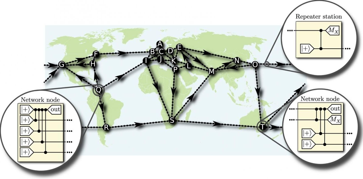
(Phys.org)—One of the most ambitious endeavors in quantum physics right now is to build a large-scale quantum network that could one day span the entire globe. In a new study, physicists have shown that describing quantum networks in a new way—as mathematical graphs—can help increase the distance that quantum information can be transmitted. Compared to classical networks, quantum networks have potential advantages such as better security and being faster under certain circumstances.

“A worldwide network may appear quite similar to the internet—a huge number of devices connected in a way that allows the exchange of information between any of them,” coauthor Michael Epping, a physicist at the University of Waterloo in Canada, told Phys.org. “But the crucial difference is that the laws of quantum theory will be dominant for the description of that information. For example, the state of the fundamental information carrier can be a superposition of the basis states 0 and 1. By now, several advantages in comparison to classical information are known, such as prime number factorization and secret communication. However, the biggest benefit of quantum networks might well be discovered by future research in the rapidly developing field of theory.”

Quantum networks involve sending entangled particles across long distances, which is challenging because particle loss and decoherence tend to scale exponentially with the distance.

Read more

Nice.


Optica l quantum technologies are based on the interactions of atoms and photons at the single-particle level, and so require sources of single photons that are highly indistinguishable – that is, as identical as possible. Current single-photon sources using semiconductor quantum dots inserted into photonic structures produce photons that are ultrabright but have limited indistinguishability due to charge noise, which results in a fluctuating electric field. Conversely, parametric down conversion sources yield photons that while being highly indistinguishable have very low brightness. Recently, however, scientists at CNRS — Université Paris-Saclay, Marcoussis, France; Université Paris Diderot, Paris, France; University of Queensland, Brisbane, Australia; and Université Grenoble Alpes, CNRS, Institut Néel, Grenoble, France; have developed devices made of quantum dots in electrically-controlled cavities that provide large numbers of highly indistinguishable photons with strongly reduced charge noise that are 20 times brighter than any source of equal quality. The researchers state that by demonstrating efficient generation of a pure single photon with near-unity indistinguishability, their novel approach promises significant advances in optical quantum technology complexity and scalability.

Dr. Pascale Senellart and Phys.org discussed the paper, Near-optimal single-photon sources in the solid state, that she and her colleagues published in Nature Photonics, which reports the design and fabrication of the first optoelectronic devices made of in electrically controlled cavities that provide bright source generating near-unity indistinguishability and pure single photons. “The ideal single photon source is a device that produces light pulses, each of them containing exactly one, and no more than one, photon. Moreover, all the photons should be identical in spatial shape, wavelength, polarization, and a spectrum that is the Fourier transform of its temporal profile,” Senellart tells Phys.org. “As a result, to obtain near optimal single photon sources in an optoelectronic device, we had to solve many scientific and technological challenges, leading to an achievement that is the result of more than seven years of research.”

While quantum dots can be considered artificial atoms that therefore emit photons one by one, she explains, due to the high refractive index of any semiconductor device, most single photons emitted by the quantum dot do not exit the semiconductor and therefore cannot be used. “We solved this problem by coupling the quantum dot to a microcavity in order to engineer the electromagnetic field around the emitter and force it to emit in a well-defined mode of the optical field,” Senellart points out. “To do so, we need to position the quantum dot with nanometer-scale accuracy in the microcavity.”

Read more