Toggle light / dark theme

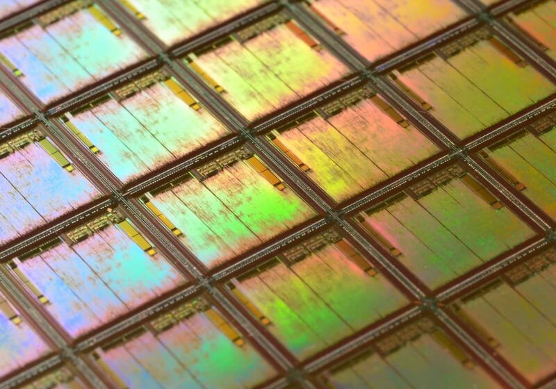
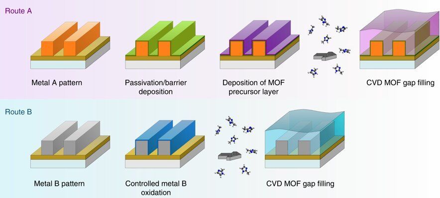
Researchers at KU Leuven and imec have successfully developed a new technique to insulate microchips. The technique uses metal-organic frameworks, a new type of materials consisting of structured nanopores. In the long term, this method can be used for the development of even smaller and more powerful chips that consume less energy. The team has received an ERC Proof of Concept grant to further their research.

Computer chips are getting increasingly smaller. That’s not new: Gordon Moore, one of the founders of chip manufacturer Intel, already predicted it in 1965. Moore’s law states that the number of transistors in a chip, or integrated circuit, doubles about every two years. This prognosis was later adjusted to 18 months, but the theory still stands. Chips are getting smaller and their processing power is increasing. Nowadays, a chip can have over a billion transistors.

But this continued reduction in size also brings with it a number of obstacles. The switches and wires are packed together so tightly that they generate more resistance. This, in turn, causes the chip to consume more energy to send signals. To have a well-functioning chip, you need an insulating substance that separates the wires from each other, and ensures that the electrical signals are not disrupted. However, that’s not an easy thing to achieve at the nanoscale level.
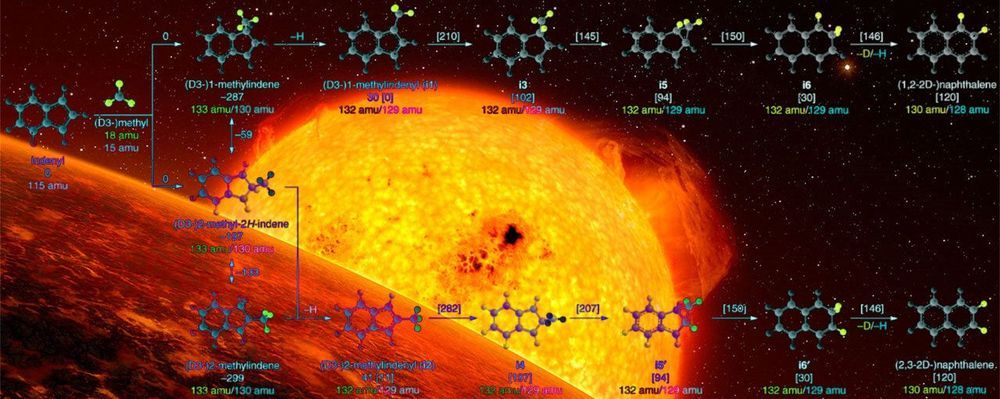
A team of scientists has discovered a new possible pathway toward forming carbon structures in space using a specialized chemical exploration technique at the Department of Energy’s Lawrence Berkeley National Laboratory (Berkeley Lab).

The team’s research has now identified several avenues by which ringed molecules known as , or PAHs, can form in space. The latest study is a part of an ongoing effort to retrace the chemical steps leading to the formation of complex carbon-containing molecules in deep space.

PAHs—which also occur on Earth in emissions and soot from the combustion of fossil fuels—could provide clues to the formation of life’s chemistry in space as precursors to interstellar nanoparticles. They are estimated to account for about 20 percent of all carbon in our galaxy, and they have the chemical building blocks needed to form 2-D and 3D carbon structures.

“Over decades, both military and space programs all around the world have known the negative impact of radiation on semiconductor-based electronics,” says Meyya Meyyappan, Chief Scientist for Exploration Technology at the Center for Nanotechnology, at NASA’s Ames Research Center. What has changed with the push towards nanoscale feature sizes is that terrestrial levels of radiation can now also cause problems that had previously primarily concerned applications in space and defence. Packaging contaminants can cause alpha radiation that create rogue electron-hole pairs, and even the ambient terrestrial neutron flux at sea level – around 20 cm−2 h−1 – can have adverse implications for nanoscale devices.

Fortunately work to produce radiation-hardy electronics has been underway for some time at NASA, where space mission electronics are particularly prone to radiation exposure and cumbersome radiation shielding comes with a particularly costly load penalty. Vacuum electronics systems, the precursors to today’s silicon world, are actually immune to radiation damage. Alongside Jin-Woo Han and colleagues Myeong-Lok Seol, Dong-Il Moon and Gary Hunter at Ames and NASA’s Glenn Research Centre, Meyyappan has been working towards a renaissance of the old technology with a nano makeover.

In a recent Nature Electronics article, they report how with device structure innovations and a new material platform they can demonstrate nanoscale vacuum channel transistors that compete with solid-state system responses while proving impervious to radiation exposure.

This would be good for hoverboards and aircrafts.


Physicists have discovered a novel quantum state of matter whose symmetry can be manipulated at will by an external magnetic field. The methods demonstrated in a series of experiments could be useful for exploring materials for next-generation nano- or quantum technologies.

Close.

Samsung is looking forward to what life might be like in the year 2069. The new report, called Samsung KX50: The Future in Focus, draws on the opinions of six of Britain’s leading academics and futurists to look at a range of new technologies that will affect people’s everyday lives.

Trying to predict the future is a dodgy business that has a notoriously low success rate. If the world of 2019 was anything like past predictions, we should have flying cars, personal jet packs, robot butlers, 100 percent atomic power producing limitless energy, little bottles containing nanobots that can grow cars on the front lawn, colonies on the Moon and Mars – and all in a society that hasn’t changed much since 1960, except it’s a bit nicer.

Truthfully, it has been some time since Moore’s law, the propensity for processors to double in transistor count every two years, has been entirely accurate. The fundamental properties of silicon are beginning to limit development and will significantly curtail future performance gains, yet with 50 years and billions invested, it seems preposterous that any ‘beyond-silicon’ technology could power the computers of tomorrow. And yet, Nano might do just that, by harnessing its ability to be designed and built like a regular silicon wafer, while using carbon to net theoretical triple performance at one-third the power.

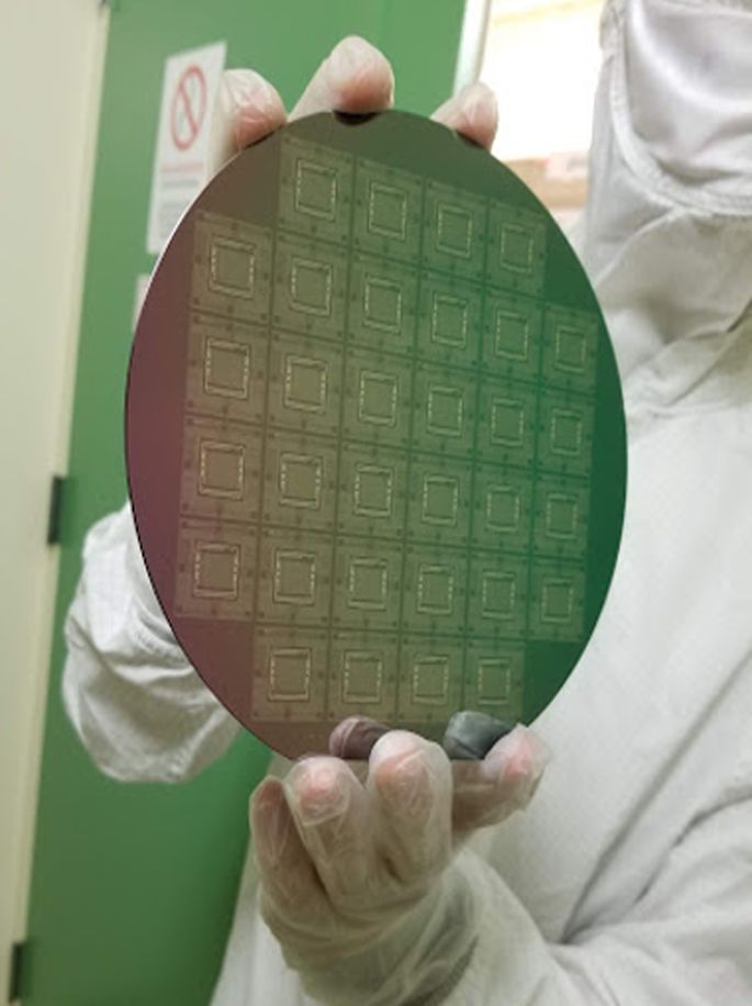
Nano began life much like all processors, a 150mm wafer with a pattern carved out of it by a regular chip fab. Dipped into a solution of carbon nanotubes bound together like microscopic spaghetti, it re-emerged with its semi-conductive carbon nanotubes stuck in the pattern of transistors and logic gates already etched on it. It then undergoes a process called ‘RINSE,’ removal of incubated nanotubes through selective exfoliation, by being coated with a polymer then dipped in a solvent. This has the effect of reducing the CNT layer to being just one tube, removing the large clumps of CNTs that stick together over 250 times more effectively than previous methods.

One of the challenges facing CNT processors has been difficulty in separating N-type and P-type transistors, which are “on” for 1 bit and “off” for 0 bit and the reverse, respectively. The difference is important for binary computing, and to perfect it, the researchers introduced ‘MIXED,’ metal interface engineering crossed with electrostatic doping. Occurring after RINSE, small platinum or titanium components are added to each transistor, then the wafer is coated in an oxide which acts as a sealant, improving performance. After that, Nano was just about done.

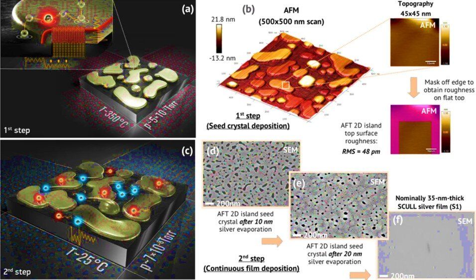
Ultra-low-loss metal films with high-quality single crystals are in demand as the perfect surface for nanophotonics and quantum information processing applications. Silver is by far the most preferred material due to low-loss at optical and near infrared (near-IR) frequencies. In a recent study now published on Scientific Reports, Ilya A. Rodionov and an interdisciplinary research team in Germany and Russia reported a two-step approach for electronic beam evaporation of atomically smooth single crystalline metal films. They proposed a method to establish thermodynamic control of the film growth kinetics at the atomic level in order to deposit state-of-the-art metal films.

The researchers deposited 35 to 100 nm thick, single-crystalline silver with sub-100 picometer (pm) with theoretically limited optical losses to form ultrahigh-Q nanophotonic devices. They experimentally estimated the contribution of material purity, material grain boundaries, surface roughness and crystallinity to the optical properties of metal films. The team demonstrated a fundamental two-step approach for single-crystalline growth of silver, gold and aluminum films to open new possibilities in nanophotonics, biotechnology and superconductive quantum technologies. The research team intends to adopt the method to synthesize other extremely low-loss single-crystalline metal films.

Optoelectronic devices with plasmonic effects for near-field manipulation, amplification and sub-wavelength integration can open new frontiers in nanophotonics, quantum optics and in quantum information. Yet, the ohmic losses associated in metals are a considerable challenge to develop a variety of useful plasmonic devices. Materials scientists have devoted research efforts to clarify the influence of metal film properties to develop high performance material platforms. Single-crystalline platforms and nanoscale structural alterations can prevent this problem by eliminating material-induced scattering losses. While silver is one of the best known plasmonic metals at optical and near-IR frequencies, the metal can be challenging for single-crystalline film growth.

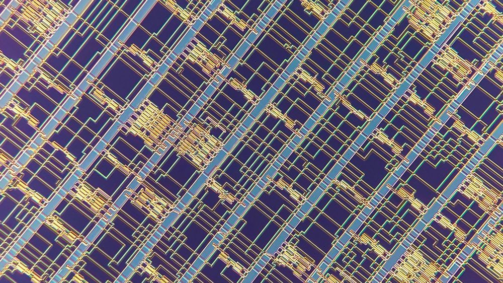
Credit: MIT Credit: MIT Engineers from the MIT and Analog Devices have created the most complex chip design yet that uses transistors made of carbon nanotubes instead of silicon. The chip was manufactured using new technologies proven to work in a commercial chip-manufacturing facility.

The researchers seem to have chosen the RISC-V instruction set architecture (ISA) for the design of the chip, presumably due to the open source nature that didn’t require hassling with licensing restrictions and costs. The RISC-V processor handles 32-bit instructions and does 16-bit memory addressing. The chip is not meant to be used in mainstream devices quite yet, but it’s a strong proof of concept that can already run “hello world”-type applications.

One advantage transistors made out of carbon nanotubes have over silicon transistors is that they can be manufactured in multiple layers, allowing for very dense 3D chip designs. DARPA also believes that carbon nanotubes may allow for the manufacturing of future 3D chips that have performance similar or better than silicon chips, but they can also be manufactured for much lower costs.