Toggle light / dark theme

The accelerator-on-a-chip demonstrated in Science is just a prototype, but Vuckovic said its design and fabrication techniques can be scaled up to deliver particle beams accelerated enough to perform cutting-edge experiments in chemistry, materials science and biological discovery that don’t require the power of a massive accelerator.

“The largest accelerators are like powerful telescopes. There are only a few in the world and scientists must come to places like SLAC to use them,” Vuckovic said. “We want to miniaturize accelerator technology in a way that makes it a more accessible research tool.”

Team members liken their approach to the way that computing evolved from the mainframe to the smaller but still useful PC. Accelerator-on-a-chip technology could also lead to new cancer radiation therapies, said physicist Robert Byer, a co-author of the Science paper. Again, it’s a matter of size.

Today, medical X-ray machines fill a room and deliver a beam of radiation that’s tough to focus on tumors, requiring patients to wear lead shields to minimize collateral damage.


On a hillside above Stanford University, the SLAC National Accelerator Laboratory operates a scientific instrument nearly 2 miles long. In this giant accelerator, a stream of electrons flows through a vacuum pipe, as bursts of microwave radiation nudge the particles ever-faster forward until their velocity approaches the speed of light, creating a powerful beam that scientists from around the world use to probe the atomic and molecular structures of inorganic and biological materials.

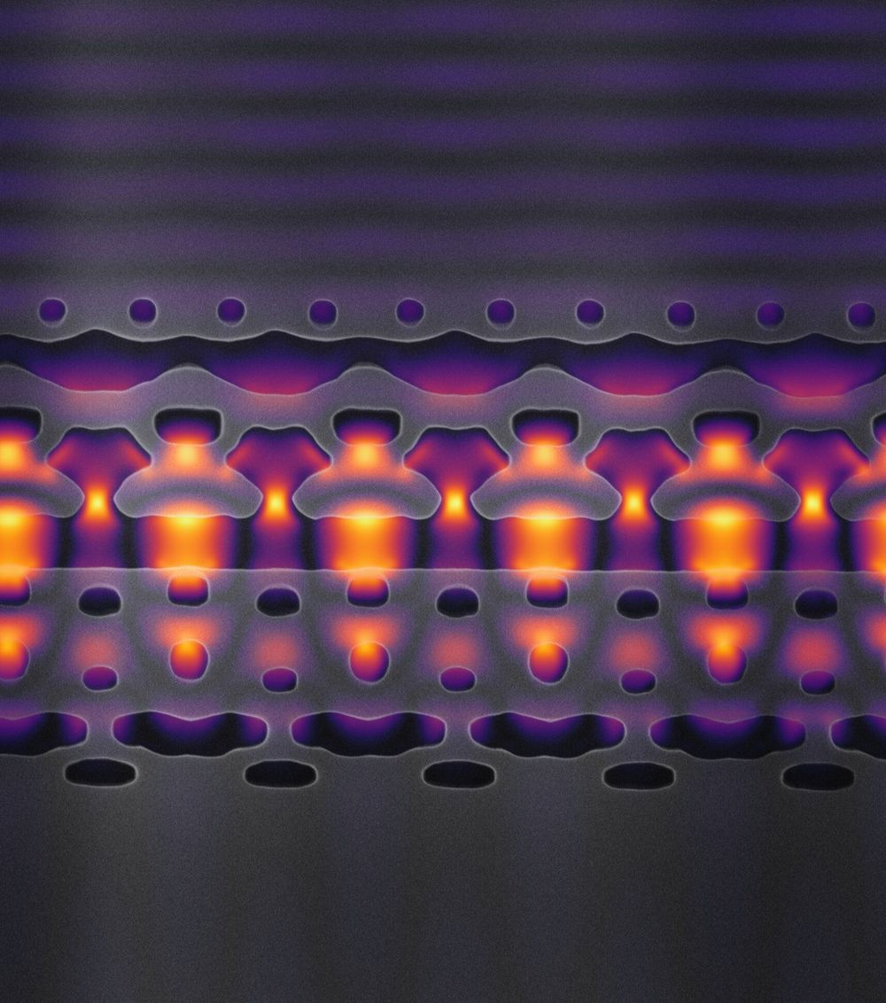
Now, for the first time, scientists at Stanford and SLAC have created a that can accelerate electrons—albeit at a fraction of the velocity of that massive instrument—using an infrared laser to deliver, in less than a hair’s width, the sort of energy boost that takes microwaves many feet.

Writing in the Jan. 3 issue of Science, a team led by electrical engineer Jelena Vuckovic explained how they carved a nanoscale channel out of silicon, sealed it in a vacuum and sent electrons through this cavity while pulses of infrared light—to which silicon is as transparent as glass is to visible light—were transmitted by the channel walls to speed the electrons along.
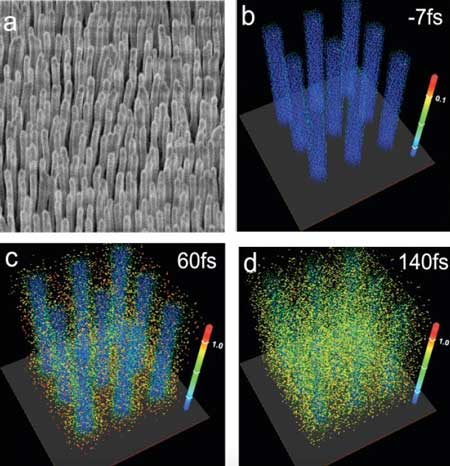
Nuclear fusion, the process that powers our sun, happens when nuclear reactions between light elements produce heavier ones. It’s also happening — at a smaller scale — in a Colorado State University laboratory.

Using a compact but powerful laser to heat arrays of ordered nanowires, CSU scientists and collaborators have demonstrated micro-scale nuclear fusion in the lab. They have achieved record-setting efficiency for the generation of neutrons — chargeless sub-atomic particles resulting from the fusion process.

Their work is detailed in a paper published in Nature Communications (“Micro-scale fusion in dense relativistic nanowire array plasmas”), and is led by Jorge Rocca, University Distinguished Professor in electrical and computer engineering and physics. The paper’s first author is Alden Curtis, a CSU graduate student.

A group of scientists from the Russian Academy of Sciences (ICG SB RAS) and the TSU Biological Institute has established a path through which nanoparticles of viruses and organic and inorganic substances from the environment enter the brain. Additionally, the researchers report a simple and inexpensive way to block their entry. The data obtained by the project could play a large role in medicine and pharmaceuticals, where nanoparticles are increasingly used for the diagnosis and treatment of serious diseases.

“There are a large number of nanoparticles of a wide variety of chemical elements and their compounds in the environment, ranging from harmless to toxic, for example, heavy metal oxides,” says Mikhail Moshkin, director of the Center for Laboratory Animal Genetic Resources of the ICG SB RAS. “Scientists have accumulated data that indicate the adverse effect of nanoparticles, for example, people who live closer than 50 meters to large highways may develop neurodegenerative diseases (Alzheimer’s, Parkinson’s and others) due to the accumulation of nanosized particles in the brain.”

The researchers sought to determine how nanoparticles enter the brain. They cannot penetrate through the lungs and blood vessels because the blood-brain barrier blocks them from the brain. Experiments conducted on rodents helped calculate the trajectory of the movement of nanoparticles.

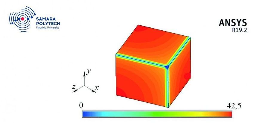
A team of scientists from the Research Center “Fundamental Problems of Thermophysics and Mechanics,” of Samara Polytech is engaged in the construction of new mathematical models and the search for methods for their study in relation to a wide range of local nonequilibrium transport processes in various physical systems. An innovative approach developed not so long ago is based on a modern version of third-generation thermodynamics. The project of these scientists, “Development, theoretical research and experimental verification of mathematical models of oscillatory processes, heat and mass transfer and thermomechanics with two- and multiphase delays” was among the winners of the RFBR contest. Recent research results are published in the journal Physica A: Statistical Mechanics and its Applications.

An interest in studying local nonequilibrium processes that take into account the specifics of transport processes at the molecular level (the mean free path of a molecule, the momentum transfer rate, relaxation time, etc.) is dictated by the need to conduct various physical processes under —for example, femtosecond concentrated exposure to energy flows on matter, ultra-low and ultra-high temperatures and pressures, shock waves, etc. Such physical processes are widely used to create new technologies for producing nanomaterials and coatings with unique physicochemical properties that cannot be obtained by traditional methods (binary and multicomponent metal alloys, ceramics, polymeric materials, metal and semiconductor glasses, nanofilms, graphene, composite nanomaterials, etc.).

“Classical thermodynamics is not suitable for describing processes that occur under local nonequilibrium conditions, since it is based on the principle of local equilibrium. Our project is important both for and for practical applications,” explains the project manager, Professor Igor Kudinov. “To accomplish the tasks, we plan to create a new, unparalleled software package designed for 3D modeling of high-speed local nonequilibrium processes of heat, mass and momentum transfer. Thus, our method opens up wide possibilities for studying processes that are practically significant from the point of view of modern nanotechnology.”

At Roswell we have developed the first Molecular Electronics chip. We utilized advances in semiconductor technology, nano-fabrication and bio-sensors to create standard CMOS chips that directly integrate sensor molecules into the CMOS integrated circuits.

Going “on-chip” to deploy bio-sensors provides unprecedented economics, precision, portability, and scalability. Our first chip is designed to read DNA; future chips will be designed for protein detection and other diverse bio-sensing applications.

For the first time, researchers and scientists from the University of Bristol, in collaboration with the Technical University of Denmark (DTU), have achieved quantum teleportation between two computer chips. The team successfully developed chip-scale devices that are able to harness the applications of quantum physics by generating and manipulating single particles of light within programmable nano-scale circuits.

Unlike regular or science fiction teleportation which transfer particles from one place to another, with quantum teleportation, nothing physical is being transported. Rather, the information necessary to prepare a target system in the same quantum state as the source system is transmitted from one location to another, with the help of classical communication and previously shared quantum entanglement between the sending and receiving location.

In a feat that opens the door for quantum computers and quantum internet, the team managed to send information from one chip to another instantly without them being physically or electronically connected. Their work, published in the journal Nature Physics, contains a range of other quantum demonstrations. This chip-to-chip quantum teleportation was made possible by a phenomenon called quantum entanglement. The entanglement happens between two photons (two light particles) with the interaction taking place for a brief moment and the two photons sharing physical states. Quantum entanglement phenomenon is so strange that physicist Albert Einstein famously described it as ‘spooky action at a distance’.

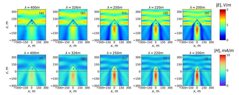
An international research group has applied methods of theoretical physics to investigate the electromagnetic response of the Great Pyramid to radio waves. Scientists predicted that under resonance conditions, the pyramid can concentrate electromagnetic energy in its internal chambers and under the base. The research group plans to use these theoretical results to design nanoparticles capable of reproducing similar effects in the optical range. Such nanoparticles may be used, for example, to develop sensors and highly efficient solar cells. The study was published in the Journal of Applied Physics.

While Egyptian are surrounded by many myths and legends, researchers have little scientifically reliable information about their physical properties. Physicists recently took an interest in how the Great Pyramid would interact with electromagnetic waves of a resonant length. Calculations showed that in the resonant state, the pyramid can concentrate in the its internal chambers as well as under its base, where the third unfinished chamber is located.

These conclusions were derived on the basis of numerical modeling and analytical methods of physics. The researchers first estimated that resonances in the pyramid can be induced by radio waves with a length ranging from 200 to 600 meters. Then they made a model of the electromagnetic response of the pyramid and calculated the extinction cross section. This value helps to estimate which part of the incident wave energy can be scattered or absorbed by the pyramid under resonant conditions. Finally, for the same conditions, the scientists obtained the electromagnetic field distribution inside the pyramid.

An international joint research team led by NIMS succeeded in fabricating a neuromorphic network composed of numerous metallic nanowires. Using this network, the team was able to generate electrical characteristics similar to those associated with higher-order brain functions unique to humans, such as memorization, learning, forgetting, becoming alert and returning to calm. The team then clarified the mechanisms that induced these electrical characteristics.

The development of artificial intelligence (AI) techniques has been rapidly advancing in recent years and has begun impacting our lives in various ways. Although AI processes information in a manner similar to the human brain, the mechanisms by which human brains operate are still largely unknown. Fundamental brain components, such as neurons and the junctions between them (synapses), have been studied in detail. However, many questions concerning the brain as a collective whole need to be answered. For example, we still do not fully understand how the brain performs such functions as memorization, learning, and forgetting, and how the brain becomes alert and returns to calm. In addition, live brains are difficult to manipulate in experimental research. For these reasons, the brain remains a mysterious organ.

A new study led by NIMS researchers reveals that, in solid electrolytes, a Si anode composed only of commercial Si nanoparticles prepared by spray deposition – the method is a cost-effective, atmospheric technique – exhibits excellent electrode performance, which has previously been observed only for film electrodes prepared by evaporation processes. This new result therefore suggests that a low-cost and large-scale production of high-capacity anodes for use in all-solid-state Li batteries is possible.

Any comments?


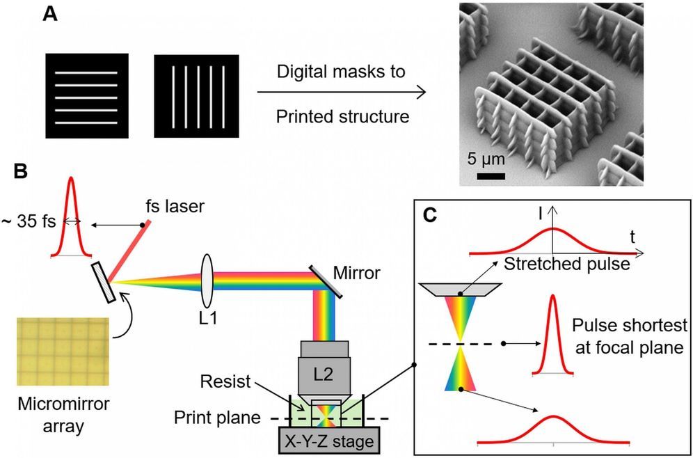
Ultraprecise 3D printing technology is a key enabler for manufacturing precision biomedical and photonic devices. However, the existing printing technology is limited by its low efficiency and high cost. Professor Shih-Chi Chen and his team from the Department of Mechanical and Automation Engineering, The Chinese University of Hong Kong (CUHK), collaborated with the Lawrence Livermore National Laboratory to develop the Femtosecond Projection Two-photon Lithography (FP-TPL) printing technology.

By controlling the spectrum via temporal focusing, the laser 3D printing process is performed in a parallel layer-by-layer fashion instead of point-by-point writing. This new technique substantially increases the printing speed by 1,000—10,000 times, and reduces the cost by 98 percent. The achievement has recently been published in Science, affirming its technological breakthrough that leads nanoscale 3D printing into a new era.

The conventional nanoscale 3D , i.e., two-photon polymerization (TPP), operates in a point-by-point scanning fashion. As such, even a centimeter-sized object can take several days to weeks to fabricate (build rate ~ 0.1 mm3/hour). The process is time-consuming and expensive, which prevents practical and industrial applications. To increase speed, the resolution of the finished product is often sacrificed. Professor Chen and his team have overcome the challenging problem by exploiting the concept of temporal focusing, where a programmable femtosecond light sheet is formed at the focal plane for parallel nanowriting; this is equivalent to simultaneously projecting millions of laser foci at the , replacing the traditional method of focusing and scanning laser at one point only. In other words, the FP-TPL technology can fabricate a whole plane within the time that the point-scanning system fabricates a point.