Toggle light / dark theme

Abstract: In 1959 renowned physicist Richard Feynman, in his talk “Plenty of Room at the Bottom,” spoke of a future in which tiny machines could perform huge feats. Like many forward-looking concepts, his molecule and atom-sized world remained for years in the realm of science fiction.

And then, scientists and other creative thinkers began to realize Feynman’s nanotechnological visions.

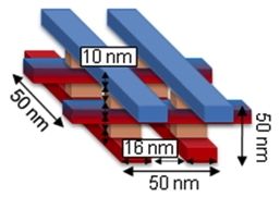
In the spirit of Feynman’s insight, and in response to the challenges he issued as a way to inspire scientific and engineering creativity, electrical and computer engineers at UC Santa Barbara have developed a design for a functional nanoscale computing device. The concept involves a dense, three-dimensional circuit operating on an unconventional type of logic that could, theoretically, be packed into a block no bigger than 50 nanometers on any side.
Read more

To all those who said it couldn’t happen for another 10+ years; this article is definitely for you.

Robert Wolkow, University of Alberta

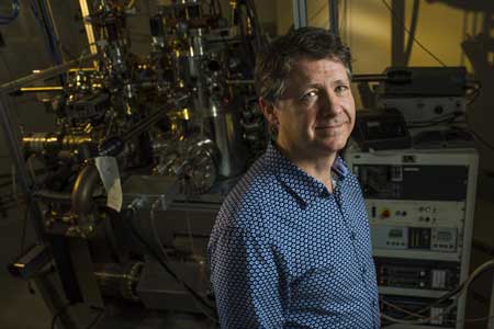
Robert Wolkow, University of Alberta physics professor and the Principal Research Officer at Canada’s National Institute for Nanotechnology, has developed a technique to switch a single-atom channel.

What does it all mean? With applications for practical systems like silicon semi-conductor electronics, it means smaller, more efficient, more energy-conserving computers, as just one example of the technology revolution that is unfolding right before our very eyes (if you can squint that hard).

Read more

New method for information storage via QC uncovered.


Abstract: Researchers from the Harvard John A. Paulson School of Engineering and Applied Sciences (SEAS) have made a discovery that could lay the foundation for quantum superconducting devices. Their breakthrough solves one the main challenges to quantum computing: how to transmit spin information through superconducting materials.

Every electronic device — from a supercomputer to a dishwasher — works by controlling the flow of charged electrons. But electrons can carry so much more information than just charge; electrons also spin, like a gyroscope on axis.

Harnessing electron spin is really exciting for quantum information processing because not only can an electron spin up or down — one or zero — but it can also spin any direction between the two poles. Because it follows the rules of quantum mechanics, an electron can occupy all of those positions at once. Imagine the power of a computer that could calculate all of those positions simultaneously.

Read more

Another article on the QC advancement; however, as I told folks synthetic diamonds are key plus the crystalized formation are proven to be very useful not only in QC processing; but also for the light-based (Quantum) networking. I see this only the beginning (as we have seen with Synthetic DNA data storage) for synthetic gem crystalize formations in their usage in technology. Hoping folks are checking out the 3D Printers creating these synthetics because we truly are on the path of seeing our world transform to new levels never imagined.


Abstract: By forcefully embedding two silicon atoms in a diamond matrix, Sandia researchers have demonstrated for the first time on a single chip all the components needed to create a quantum bridge to link quantum computers together.

“People have already built small quantum computers,” says Sandia researcher Ryan Camacho. “Maybe the first useful one won’t be a single giant quantum computer but a connected cluster of small ones.”

Distributing quantum information on a bridge, or network, could also enable novel forms of quantum sensing, since quantum correlations allow all the atoms in the network to behave as though they were one single atom.

Read more

Breaks through the 5-nanometer quantum tunneling threshold; may allow for Moore’s law to continue…


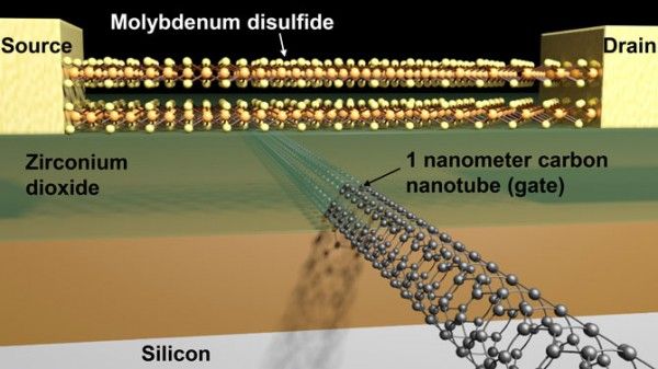
Schematic of a transistor with molybdenum disulfide semiconductor and 1-nanometer carbon nanotube gate. (credit: Sujay Desai/Berkeley Lab)

The first transistor with a working 1-nanometer (nm) gate has been created by a team led by Lawrence Berkeley National Laboratory (Berkeley Lab) scientists. Until now, a transistor gate size less than 5 nanometers has been considered impossible because of quantum tunneling effects. (One nanometer is the diameter of a glucose molecule.)

The breakthrough was achieved by creating a 2D (flat) semiconductor field-effect transistor using molybdenum disulfide (MoS2) instead of silicon and a 1D single-walled carbon nanotube (SWCNT) as a gate electrode, instead of various metals. (SWCNTs are hollow cylindrical tubes with diameters as small as 1 nanometer.)

Read more

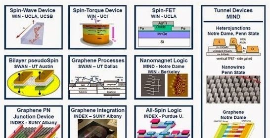
Eurolab HPC tries to assess the future disruptive technology for high performance computing beyond Exascale computers.

They survey the currents state of research and development and its potential for the future of the following hardware technologies:

CMOS scaling
Die stacking and 3D chip technologies
Non-volatile Memory (NVM) technologies
Photonics
Resistive Computing
Neuromorphic Computing
Quantum Computing
Nanotubes
Graphene and
Diamond Transistors

Read more