Toggle light / dark theme

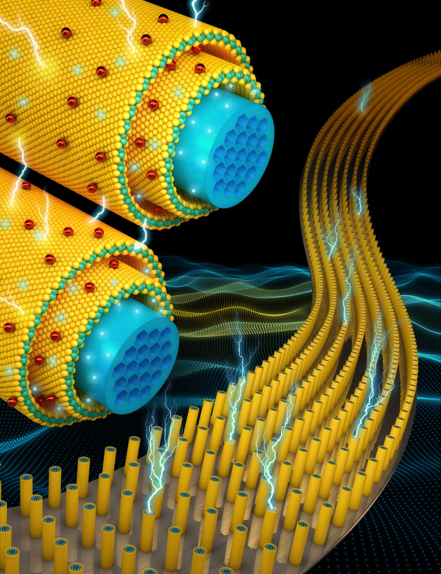
Illustration representing the novel design of a hybrid supercapacitor, showing bundles of nanowires (blue) coated with 2D energy-storage materials (yellow) (credit: University of Central Florida)

University of Central Florida researchers have developed a radical new supercapacitor design that could one day replace lithium-ion batteries, allowing users to charge a mobile phone in a few seconds and with a charge that lasts a week, according to the researchers. The new battery would be flexible and a fraction of the size of a lithium-ion battery.

The proof-of-concept design is based on a hybrid supercapacitor composed of a core with millions of highly conductive nanowires coated with shells of two-dimensional materials. It combines fast charging and discharging (high power density) and high storage capacity (high energy density).

Read more

Machines lace almost all social, political cultural and economic issues currently being discussed. Why, you ask? Clearly, because we live in a world that has all its modern economies and demographic trends pivoting around machines and factories at all scales.

We have reached the stage in the evolution of our civilization where we cannot fathom a day without the presence of machines or automated processes. Machines are not only used in sectors of manufacturing or agriculture but also in basic applications like healthcare, electronics and other areas of research. Although, machines of varying types had entered the industrial landscape long ago, technologies like nanotechnology, the Internet of Things, Big Data have altered the scenario in an unprecedented manner.

The fusion of nanotechnology with conventional mechanical concepts gives rise to the perception of ‘molecular machines’. Foreseen to be a stepping stone into nano-sized industrial revolution, these microscopic machines are molecules designed with movable parts that behave in a way that our regular machines operate in. A nano-scale motor that spins in a given direction in presence of directed heat and light would be an example of a molecular machine.

Read more

Terahertz (THz) radiation is used today most prominently for security screening at the airport. It’s the machine you stand in with your hands up as it swings its scanning arms in front and behind you. In medicine, terahertz imaging has the potential to help diagnoze certain types of cancer and to monitor a variety of health parameters to aid in assessment of overall health. Because of the extremely short length of terahertz waves, this imaging modality has a lot of limitations, including shallow penetration into tissues, and that prevents it from being used more widely. Yet, since it’s non-ionising, it’s probably safe and may even replace dangerous X-rays for some applications.

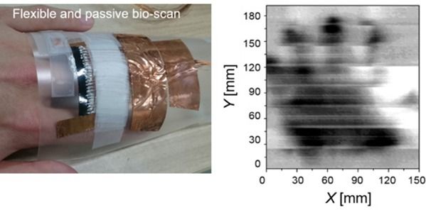
Currently, terahertz imaging is very poor at scanning curved surfaces even though it can peer a few millimeters deep into some tissues. To overcome this, researchers at Tokyo Institute of Technology have developed a flexible and even wearable terahertz scanner that can image curved 3D surfaces such as our skin.

Made of 23 carbon nanotube detectors that work as a unified imaging array, their device can be wrapped around a finger, for example. Because carbon nanotubes are able to absorb a wide range of terahertz radiation, there’s no need for planar antennas.

Read more

Lenses with a surface accuracy in the nanometer range are behind ever more accurate laser and optical systems. Manufacturers depend on ultra-precise optical and mechanical ablation processes, innovative coating processes and extremely accurate measuring technology to venture into these nano-worlds. The latest trends in optical manufacturing will be showcased by the world’s leading trade fair LASER World of PHOTONICS, from June 26–29, 2017 in Munich.

Nanoscribe GmbH’s 3D printing process creates three-dimensional micro and nano lenses from photosensitive coatings Nanoscribe GmbH’s 3D printing process creates three-dimensional micro and nano lenses from photosensitive coatings. The structures are built up a pulse at a time by highly focused femtosecond lasers employing two-photon polymerization. Source: Nanoscribe GmbH

The diversity of lenses, their shapes, sizes and materials is growing all the time. Applications in non-visible wavelengths from x-rays and ultraviolet to the far infrared also require special optics, such as material processing using short pulse and ultrashort pulse lasers or imaging techniques in the medical and research fields and industrial quality control.

Read more

Immensely concentrated sunlight provides a novel method for the synthesis of many nanomaterials that possess remarkable photonic, tribological, electronic, and catalytic properties.

The solar paradigm of creating singular nanomaterials that possess unprecedented photonic, tribological, electronic, and catalytic properties is arguably far less familiar than the energy-saving paradigms of solar photovoltaics and solar thermal systems. Much of the research in this field has evolved over the past decade from our collaborations (i.e., between researchers at Ben-Gurion University of the Negev and the Weizmann Institute of Science, Israel).

Read more

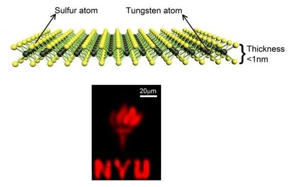
Research out of New York University’s Tandon School of Engineering has found a new method for developing electronics at the atomic scale — and it’s difficult to get much smaller than that.

Scientists and engineers have previously tried developing electronics using two-dimensional or monolayer electronic materials like graphene to make transistors, but found that the material’s lack of an energy band gap poses difficulties for semiconductor applications.

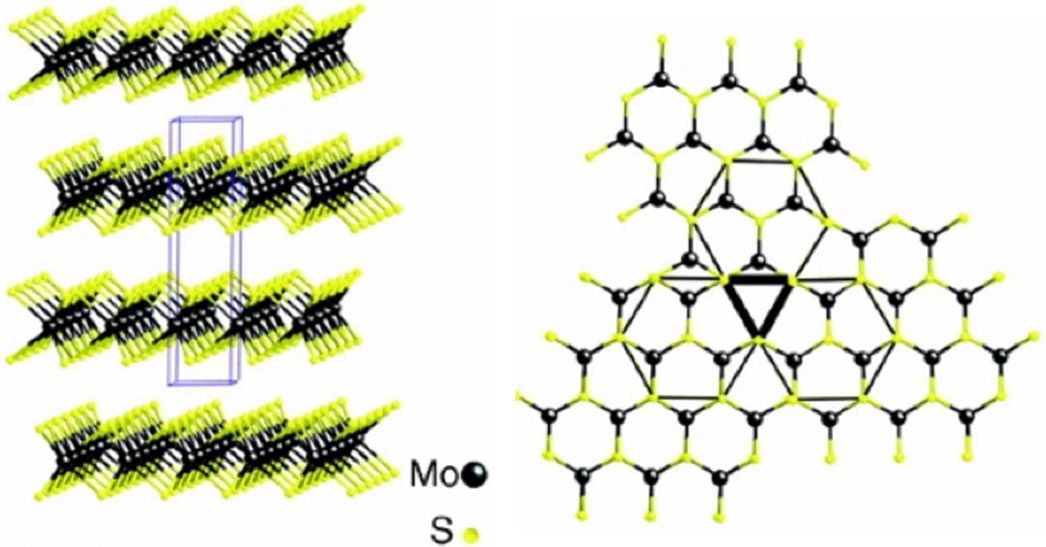
The new research by assistant professor of electrical and computer engineering Davood Shahrjerdi and doctoral student Abdullah Alharbi, has shown that using a monolayer of tungsten disulfide might be the key to unlocking the potential in nano-scale electronics.

Read more

Researchers from Case Western Reserve University, Dayton Air Force Research Laboratory and China have developed a new dry adhesive that bonds in extreme temperatures—a quality that could make the product ideal for space exploration and beyond.

The gecko-inspired adhesive loses no traction in temperatures as cold as liquid nitrogen or as hot as molten silver, and actually gets stickier as heat increases, the researchers report.

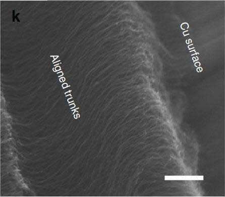
The research, which builds on earlier development of a single-sided dry adhesive tape based on vertically aligned carbon nanotubes, is published in the journal Nature Communications (“Carbon nanotube dry adhesives with temperature-enhanced adhesion over a large temperature range”). As far as the researchers know, no other dry adhesive is capable of working at such temperature extremes.

Read more

With bots the size of a single blood cell, this could spur a huge leap in the field of non-invasive surgeries.

Scientists have developed the world’s first light-seeking synthetic nanorobot which may help surgeons remove tumours and enable more precise engineering of targeted medications.

It has been a dream in science fiction for decades that tiny robots can fundamentally change our daily life. The famous science fiction movie “Fantastic Voyage” is a very good example, with a group of scientists driving their miniaturised Nano-submarine inside human body to repair a damaged brain.

Read more

Tomi Laurila’s research topic has many quirky names.

‘Nanodiamond, nanohorn, nano-onion…’ lists off the Aalto University Professor, recounting the many nano-shapes of carbon. Laurila is using these shapes to build new materials: tiny sensors, only a few hundred nanometres across, that can achieve great things due to their special characteristics.

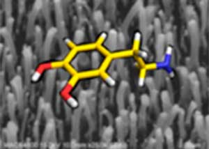
Tl.pngFor one, the sensors can be used to enhance the treatment of neurological conditions. That is why Laurila, University of Helsinki Professor Tomi Taira and experts from HUS (the Hospital District of Helsinki and Uusimaa) are looking for ways to use the sensors for taking electrochemical measurements of biomolecules. Biomolecules are e.g. neurotransmitters such as glutamate, dopamine and opioids, which are used by nerve cells to communicate with each other.

Read more

Tinier than the AIDS virus—that is currently the circumference of the smallest transistors. The industry has shrunk the central elements of their computer chips to fourteen nanometers in the last sixty years. Conventional methods, however, are hitting physical boundaries. Researchers around the world are looking for alternatives. One method could be the self-organization of complex components from molecules and atoms. Scientists at the Helmholtz-Zentrum Dresden-Rossendorf (HZDR) and Paderborn University have now made an important advance: the physicists conducted a current through gold-plated nanowires, which independently assembled themselves from single DNA strands. Their results have been published in the scientific journal Langmuir.

At first glance, it resembles wormy lines in front of a black background. But what the electron microscope shows up close is that the nanometer-sized structures connect two electrical contacts. Dr. Artur Erbe from the Institute of Ion Beam Physics and Materials Research is pleased about what he sees. “Our measurements have shown that an electrical current is conducted through these tiny wires.” This is not necessarily self-evident, the physicist stresses. We are, after all, dealing with components made of modified DNA. In order to produce the , the researchers combined a long single strand of genetic material with shorter DNA segments through the base pairs to form a stable double strand. Using this method, the structures independently take on the desired form.

“With the help of this approach, which resembles the Japanese paper folding technique origami and is therefore referred to as DNA-origami, we can create tiny patterns,” explains the HZDR researcher. “Extremely small circuits made of molecules and atoms are also conceivable here.” This strategy, which scientists call the “bottom-up” method, aims to turn conventional production of electronic components on its head. “The industry has thus far been using what is known as the ‘top-down’ method. Large portions are cut away from the base material until the desired structure is achieved. Soon this will no longer be possible due to continual miniaturization.” The new approach is instead oriented on nature: molecules that develop complex structures through self-assembling processes.

Read more