Toggle light / dark theme

AMERICAN telecom customers experienced widespread cellphone outages during what was believed to be the largest cyberattack in US history.

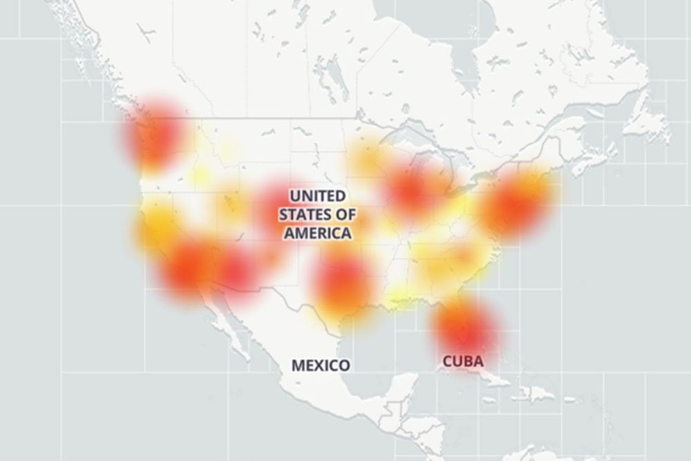
Thousands of T-Mobile, Metro by T-Mobile, AT&T, Verizon, and Sprint customers all reported outages in areas including Florida, Georgia, New York, and California on Monday afternoon.

The disruptions were part of a large-scale distributed denial-of-service, or DDoS, attack meant to overwhelm an online service with multiple traffic sources to render it unusable, according to Pop Culture.

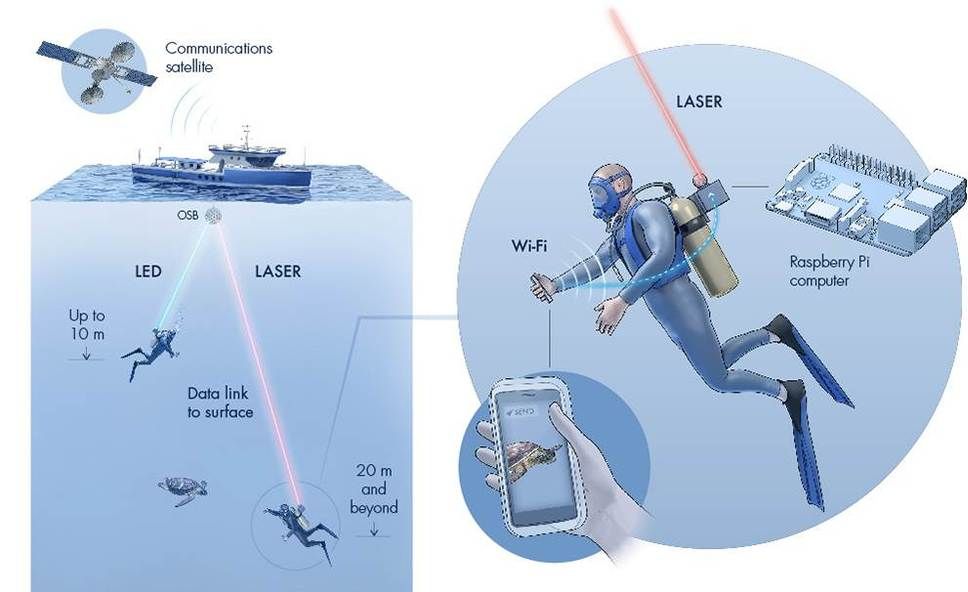
Radio waves travel poorly through the water, which makes it difficult for divers or submersibles to wirelessly transmit information to the surface. Scientists are trying to change that, though, by developing an underwater version of Wi-Fi.

Back in 2018, we heard how researchers at Saudi Arabia’s King Abdullah University of Science and Technology (KAUST) had used lasers to transmit HD video through water. Their experimental new system, known as Aqua-Fi, builds on that technology.

A user such as a scuba diver would start by sending data (such as photos or videos) from a smartphone contained in a watertight housing. That data would initially be transmitted in the form of radio waves, going just a few feet to a small device mounted on the diver’s air tanks.

Miniaturization has enabled technology like smartphones, health watches, medical probes and nano-satellites, all unthinkable a couple decades ago. Just imagine that in the course of 60 years, the transistor has shrunk from the size of your palm to 14 nanometers in dimension, 1000 times smaller than the diameter of a hair.

Miniaturization has pushed technology to a new era of optical circuitry. But in parallel, it has also triggered new challenges and obstacles, for example, controlling and guiding at the nanometer scale. Researchers are looking for techniques to confine light into extremely tiny spaces, millions of times smaller than current ones. Studies had earlier found that metals can compress light below the wavelength-scale (diffraction limit).

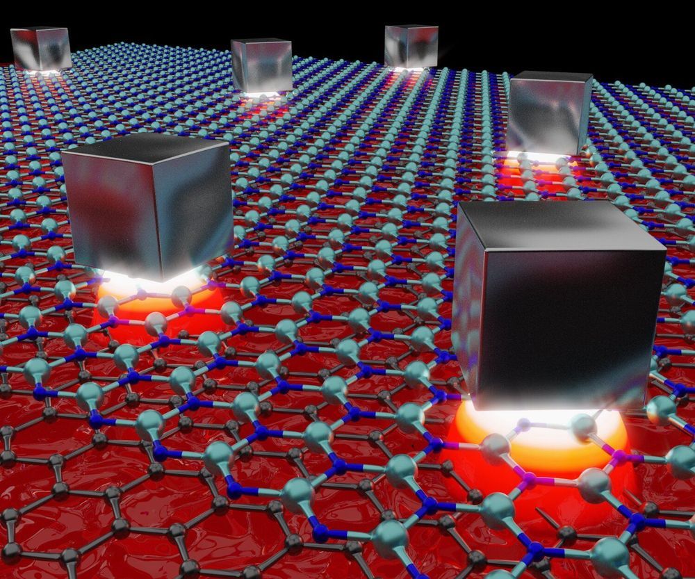
In that aspect, , a material composed from a single layer of carbon atoms, which exhibits exceptional optical and electrical properties, is capable of guiding light in the form of plasmons, which are oscillations of electrons that strongly interact with light. These graphene plasmons have a natural ability to confine light to very small spaces. However, until now, it was only possible to confine these plasmons in one direction, while the actual ability of light to interact with small particles like atoms and molecules resides in the volume into which it can be compressed. This type of confinement in all three dimensions is commonly regarded as an optical cavity.
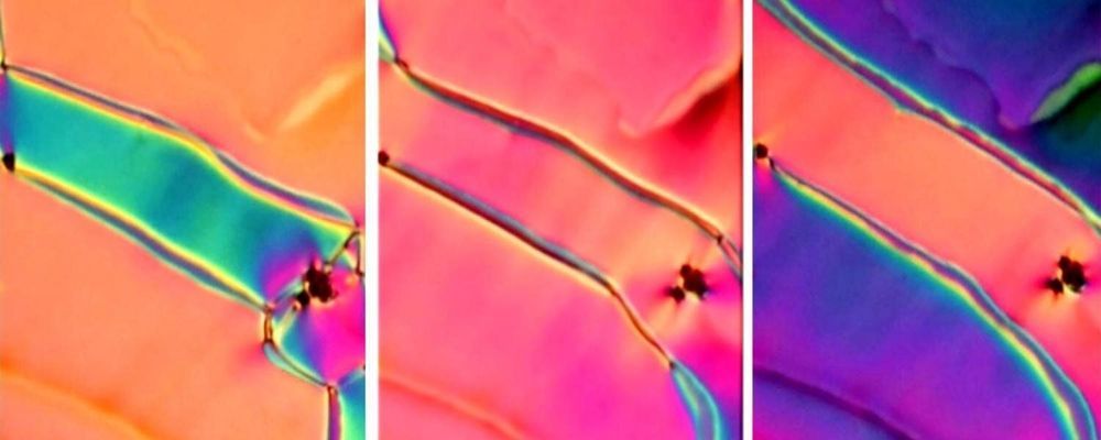
Researchers at the University of Colorado Boulder’s Soft Materials Research Center (SMRC) have discovered an elusive phase of matter, first proposed more than 100 years ago and sought after ever since.

The team describes the discovery of what scientists call a “ferroelectric nematic” phase of liquid crystal in a study published today in the Proceedings of the National Academy of Sciences. The discovery opens a door to a new universe of materials, said co-author Matt Glaser, a professor in the Department of Physics.

Nematic liquid crystals have been a hot topic in materials research since the 1970s. These materials exhibit a curious mix of fluid- and solid-like behaviors, which allow them to control light. Engineers have used them extensively to make the liquid crystal displays (LCDs) in many laptops, TVs and cellphones.

Mobile phones and computers are currently responsible for up to 8% of the electricity use in the world. This figure has been doubling each past decade but nothing prevents it from skyrocketing in the future. Unless we find a way for boosting energy efficiency in information and communications technology, that is. An international team of researchers, including Ikerbasque Research Associate Alexey Nikitin (DIPC), has just published in Nature 1 a breakthrough in quantum physics that could deliver exactly that: electronics and communications technology with ultralow energy consumption.

Future information and communication technologies will rely on the manipulation of not only electrons but also of light at the nanometer-scale. Squeezing light to such a small size has been a major goal in nanophotonics for many years. Particularly strong light squeezing can be achieved with polaritons, quasiparticles resulting from the strong coupling of photons with a dipole-carrying excitation, at infrared frequencies in two-dimensional materials, such as graphene and hexagonal boron nitride. Polaritons can be found in materials consisting of two-dimensional layers bound by weak van der Waals forces, the so-called van der Waals materials. These polaritons can be tuned by electric fields or by adjusting the material thickness, leading to applications including nanolasers, tunable infrared and terahertz detectors, and molecular sensors.

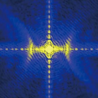
But there is a major problem: even though polaritons can have long lifetimes, they have always been found to propagate along all directions (isotropic) of the material surface, thereby losing energy quite fast, which limits their application potential.

A new version of Google’s mapping service being rolled out will display pandemic-related transit alerts and let people know when buses or trains might be crowded.

Updated versions of the free app for smartphones powered by Apple or Google-backed Android software will also let drivers know about COVID-19 checkpoints or restrictions on their routes.

“We’re introducing features to help you easily find important information if you need to venture out, whether it’s by car or public transportation,” Google Maps product management director Ramesh Nagarajan said in a blog post.

https://youtube.com/watch?v=Yi6q1j_QjSc

· 4 hrs ·

Now that they exist it certainly will change the world.


Waste heat is all around you. On a small scale, if your phone or laptop feels warm, that’s because some of the energy powering the device is being transformed into unwanted heat.

On a larger scale, electric grids, such as high power lines, lose over 5% of their energy in the process of transmission. In an electric power industry that generated more than US$400 billion in 2018, that’s a tremendous amount of wasted money.

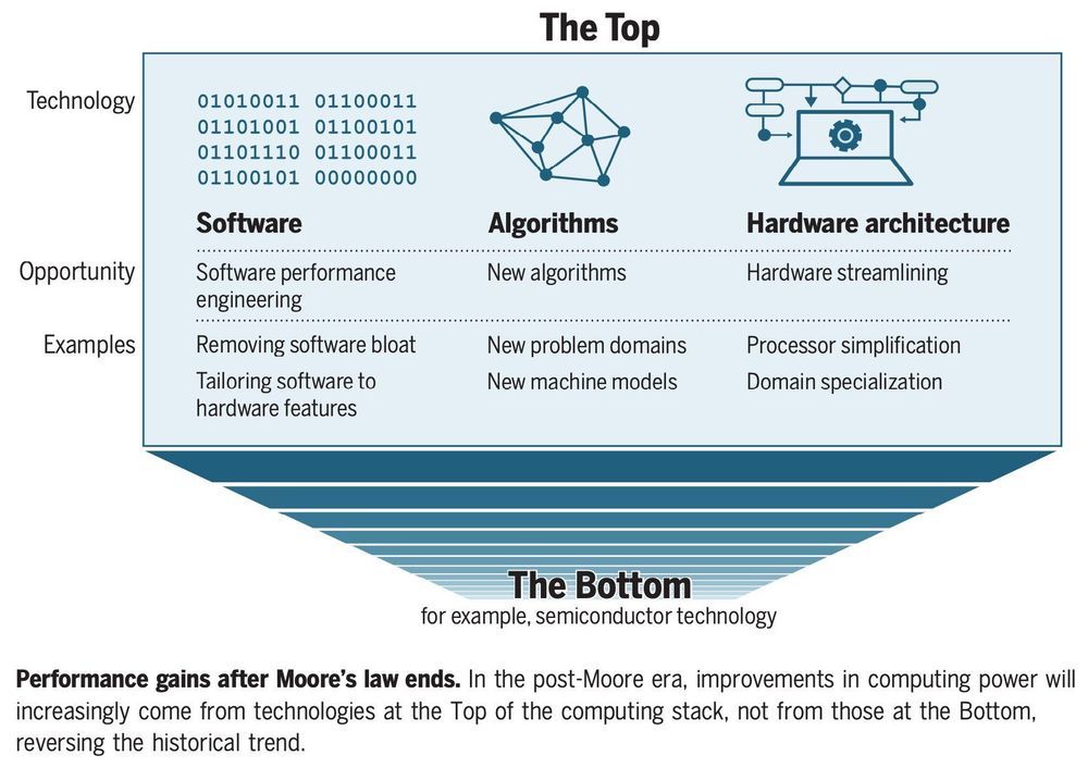
In 1965, Intel co-founder Gordon Moore predicted that the number of transistors that could fit on a computer chip would grow exponentially —- and they did, doubling about every two years. For half a century Moore’s Law has endured: computers have gotten smaller, faster, cheaper and more efficient, enabling the rapid worldwide adoption of PCs, smartphones, high-speed Internet and more.

This miniaturization trend has led to silicon chips today that have almost unimaginably small circuitry. Transistors, the tiny switches that implement computer microprocessors, are so small that 1000 of them laid end-to-end are no wider than a human hair. For a long time, the smaller the transistors were, the faster they could switch.

But today, we’re approaching the limit of how small transistors can get. As a result, over the last decade researchers have been scratching their heads to find other ways to improve performance so that the computer industry can continue to innovate.

The endeavor escalates global competition for much-sought-after semiconductor technology and is intended to build on the island’s technology industry, led by major players such as key Apple Inc. suppliers Taiwan Semiconductor Manufacturing Co. and Hon Hai Precision Industry Co. Taiwan has been caught in the middle of a clash between the U.S. and China over the development of chip technology that powers everything from smartphones to 5G base stations.


Taiwan is dangling incentives to attract more than NT$40 billion ($1.3 billion) of annual investments in research and technology, creating a seven-year blueprint to safeguard the island’s lead in semiconductors and other cutting-edge fields.

As part of the initiative, the cabinet plans to allocate more than NT$10 billion to entice foreign chipmakers to set up R&D facilities locally, confirming an earlier Bloomberg News report. The government said Thursday it aims to subsidize as much as half of all research and development costs incurred by global chip companies that build centers on the island.