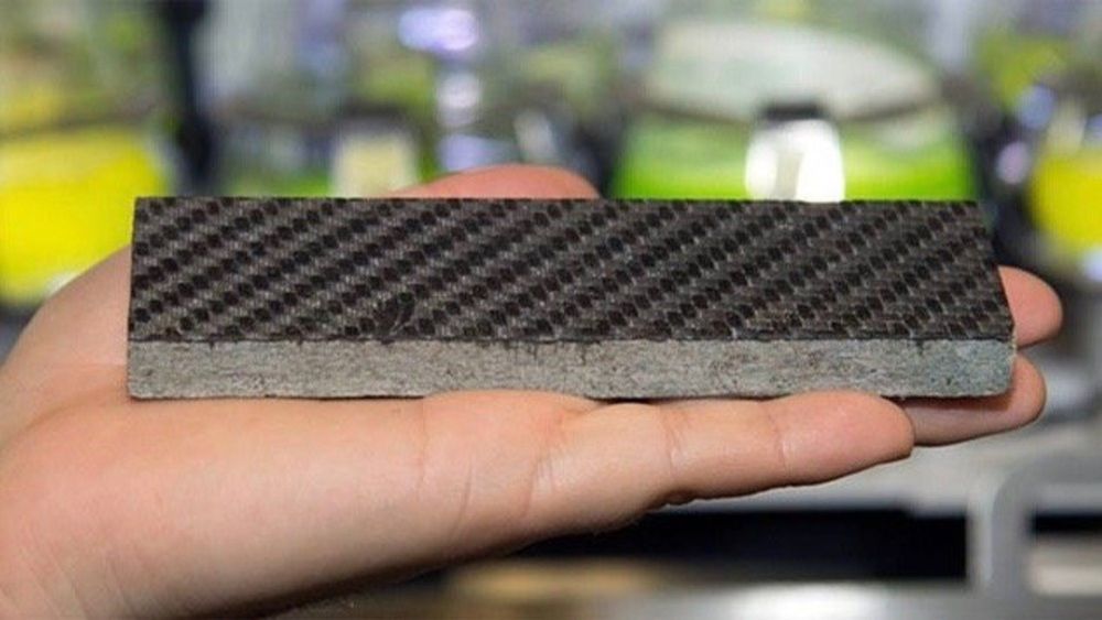
The material has two major benefits for the climate.


This could lead to euclidean geometry devices.
A system for transmission of information using a curl-free magnetic vector potential radiation field. The system includes current-carrying apparatus for generating a predominantly curl-free magnetic vector potential field coupled to apparatus for modulating the current applied to the field generating apparatus. Receiving apparatus includes a detector with observable properties that vary with the application of an applied curl-free magnetic vector potential field. Analyzing apparatus for determining the information content of modulation imposed on the curl-free vector potential field is coupled to the detector. The magnetic vector potential field can be established in materials that are not capable of transmitting more common electromagnetic radiation.

Image Credits: Thinkstock
Materials scientists are constantly working on developing stronger and better materials for various industries. Spider silk, diamond, graphene, and nanotubes have all been proved to be stronger than steel in one respect or another. Now, certain types of plastics join this list.
The following article looks at three research findings in the field of plastics.
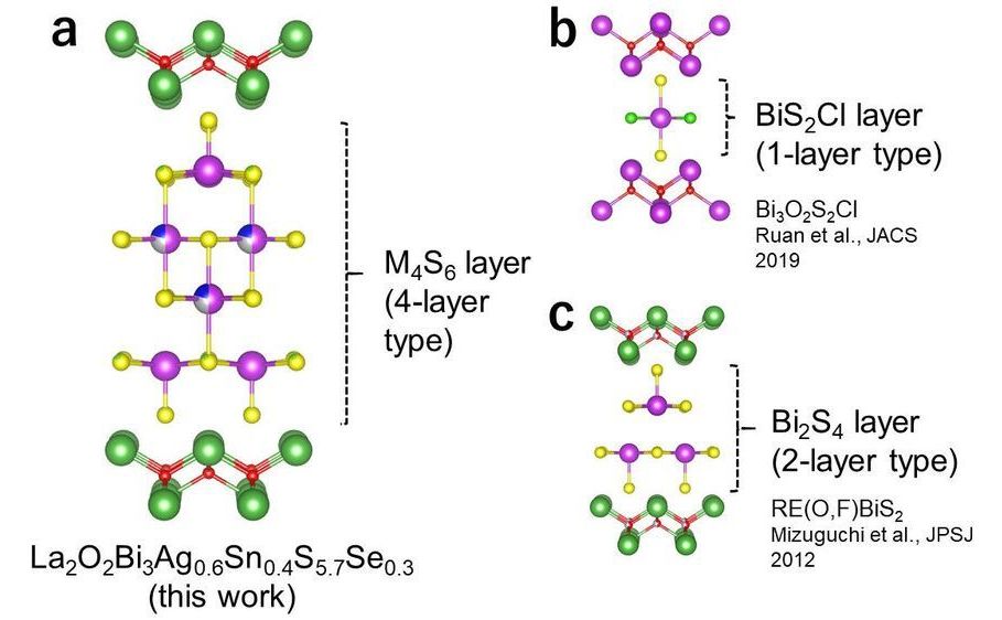
Scientists from Tokyo Metropolitan University have created a new layered superconducting material with a conducting layer made of bismuth, silver, tin, sulfur and selenium. The conducting layer features four distinct sublayers; by introducing more elements, they were able to achieve unparalleled customizability and a higher “critical temperature” below which superconductivity is observed, a key objective of superconductor research. Their design strategy may be applied to engineer new and improved superconducting materials.
Once an academic curiosity, superconductors are now at the cutting edge of real technological innovations. Superconducting magnets are seen in everyday MRI machines, particle accelerators for medical treatments, not to mention the new Chuo Shinkansen maglev train connecting Tokyo to Nagoya currently being built. Recently, a whole new class of “layered” superconducting structures have been studied, consisting of alternate layers of superconducting and insulating two-dimensional crystalline layers. In particular, the customizability of the system has garnered particular interest in light of its potential to create ultra-efficient thermoelectric devices and a whole new class of “high temperature” superconducting materials.
A team led by Associate Professor Yoshikazu Mizuguchi from Tokyo Metropolitan University recently created a bismuth sulfide based layered superconductor; their work has already revealed novel thermoelectric properties and an elevated “critical temperature” below which superconductivity is observed. Now, working with a team from the University of Yamanashi, they have taken a multi-layered version of the system, where the conducting layer consists of four atomic layers, and begun swapping out small proportions of different atomic species to probe how the material changes.
Controlling the interactions between light and matter has been a long-standing ambition for scientists seeking to develop and advance numerous technologies that are fundamental to society. With the boom of nanotechnology in recent years, the nanoscale manipulation of light has become both, a promising pathway to continue this advancement, as well as a unique challenge due to new behaviors that appear when the dimensions of structures become comparable to the wavelength of light.
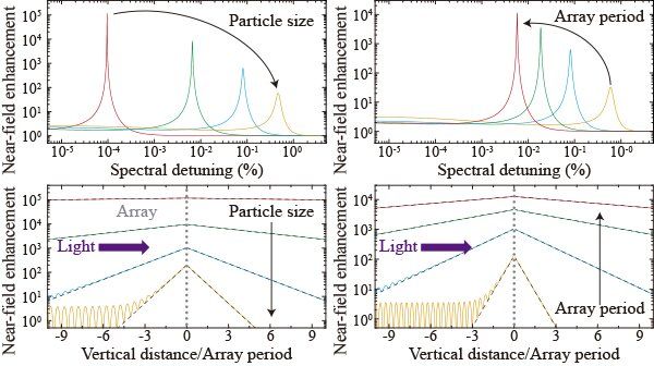
Scientists in the Theoretical Nanophotonics Group at The University of New Mexico’s Department of Physics and Astronomy have made an exciting new advancement to this end, in a pioneering research effort titled “Analysis of the Limits of the Near-Field Produced by Nanoparticle Arrays,” published recently in the journal, ACS Nano, a top journal in the field of nanotechnology. The group, led by Assistant Professor Alejandro Manjavacas, studied how the optical response of periodic arrays of metallic nanostructures can be manipulated to produce strong electric fields in their vicinity.
The arrays they studied are composed of silver nanoparticles, tiny spheres of silver that are hundreds of times smaller than the thickness of a human hair, placed in a repeating pattern, though their results apply to nanostructures made of other materials as well. Because of the strong interactions between each of the nanospheres, these systems can be used for different applications, ranging from vivid, high-resolution color printing to biosensing that could revolutionize healthcare.
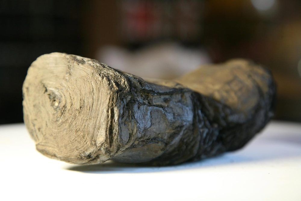
Researchers led by the renowned ancient artifacts decoder, Professor Brent Seales, will be using Diamond, the UK’s national synchrotron science facility in the heart of Oxfordshire, to examine a collection of world-famous ancient artifacts owned by the Institut de France. Using this powerful light source and special techniques the team has developed, the researchers are working to virtually unwrap two complete scrolls and four fragments from the damaged Herculaneum scrolls. After decades of effort, Seales thinks the scans from Diamond represent his team’s best chance yet to reveal the elusive contents of these 2,000-year-old papyri.
Prof Seales is director of the Digital Restoration Initiative at the University of Kentucky (US), a research program dedicated to the development of software tools that enable the recovery of fragile, unreadable texts. According to Seales, Diamond Light Source is an absolutely crucial element in our long-term plan to reveal the writing from damaged materials, as it offers unparalleled brightness and control for the images we can create, plus access to a brain trust of scientists who understand our challenges and are eager to help us succeed.?Texts from the ancient world are rare and precious, and they simply cannot be revealed through any other known process. Thanks to the opportunity to study the scrolls at Diamond Light Source, which has been made possible by the National Endowment for the Humanities and the Andrew Mellon Foundation, we are poised to take a tremendous step forward in our ability to read and visualize this material.

Hemp is a wonder crop. It’s an incredibly versatile plant that can be used for a huge range of purposes.
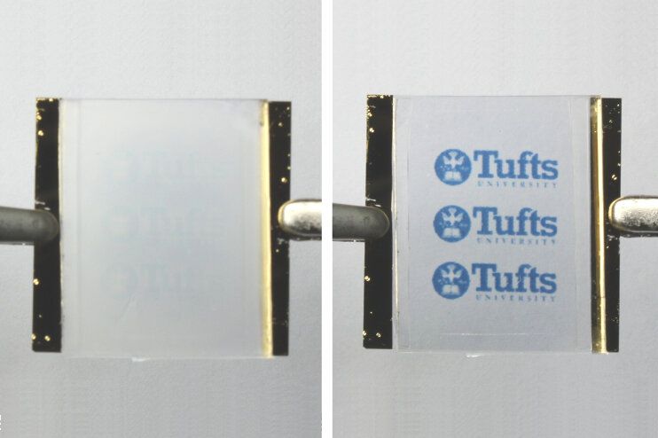
Researchers at Tufts University School of Engineering have developed silk materials that can wrinkle into highly detailed patterns—including words, textures and images as intricate as a QR code or a fingerprint. The patterns take about one second to form, are stable, but can be erased by flooding the surface of the silk with vapor, allowing the researchers to “reverse” the printing and start again. In an article published today in the Proceedings of the National Academy of Sciences, the researchers demonstrate examples of the silk wrinkle patterns, and envision a wide range of potential applications for optical electronic devices.
The smart textile takes advantage of the natural ability of silk fiber proteins—fibroin—to undergo a change of conformation in response to external conditions, including exposure to water vapor, methanol vapor and UV radiation. Water and methanol vapor, for example, can soak into the fibers and interfere with hydrogen bond cross links in the silk fibroin, causing it to partially ‘unravel’ and release tension in the fiber. Taking advantage of this property, the researchers fabricated a silk surface from dissolved fibroin by depositing it onto a thin plastic membrane (PDMS). After a cycle of heating and cooling, the silk surface of the silk/PDMS bilayer folds into nanotextured wrinkles due to the different mechanical properties of the layers.
Exposing any part of that wrinkled surface to water or methanol vapor causes the fibers to relax and the wrinkles to flatten. The smooth surface transmits more than 80% of light, while the wrinkled surface only allows 20% or less through, creating a visible contrast and the perception of a printed pattern. The surface can be selectively exposed to vapor using a patterned mask, resulting in a matched pattern in the textured silk. Patterns may also be created by depositing water using inkjet printing. The resolution of this printing method is determined by the resolution of the mask itself, or the nozzle diameter of the inkjet printer.

Another interesting aspect of The North Face’s latest fabric tech is that it developed it with sustainability in mind. The company said that every Futurelight garment will be produced at a solar-powered factory, and they’ll be made from recycled materials and will go through a process that cuts chemical consumption. In other words, not only are waterproof, lightweight and comfortable, but they’re good for the environment, as well. (Or at least, not as bad as a lot of other synthetic fabrics.)
To celebrate the launch of Futurelight, The North Face built an elaborate art installation in New York City. In it, you could see its new high-tech jackets floating underneath thinly disguised marketing messages like, “WHAT IF WATERPROOF GEAR KEPT YOU DRY INSIDE AND OUT?” and “WHAT IF BREATHABILITY IS THE BREAKTHROUGH.” There was also a giant triangle displaying images of snow-covered mountains and other outdoor scenes. Of course, it was all relevant to what The North Face is known for: making clothes for adventurous people.
The North Face’s Futurelight jacket collection is available now on its site, with the men’s Flight Series jackets starting at a cool $280. And, eventually, The North Face plans to put the technology in other gear, including tents, gloves and more.