Toggle light / dark theme

In the drive to miniaturize electronics, solenoids have become way too big, say Rice University scientists who discovered the essential component can be scaled down to nano-size with macro-scale performance.

The secret is in a spiral form of atom-thin graphene that, remarkably, can be found in nature, according to Rice theoretical physicist Boris Yakobson and his colleagues.

“Usually, we determine the characteristics for materials we think might be possible to make, but this time we’re looking at a configuration that already exists,” Yakobson said. “These spirals, or screw dislocations, form naturally in graphite during its growth, even in common coal.”

nano-coil made of graphene.

Read more

https://www.youtube.com/watch?v=W9N_Fsbngh8

During a recent United Nations meeting about emerging global risks, political representatives from around the world were warned about the threats posed by artificial intelligence and other future technologies.

The event, organized by Georgia’s UN representatives and the UN Interregional Crime and Justice Research Institute (UNICRI), was set up to foster discussion about the national and international security risks posed by new technologies, including chemical, biological, radiological, and nuclear (CBRN) materials.

The panel was also treated to a special discussion on the potential threats raised by artificial superintelligence—that is, AI whose capabilities greatly exceed those of humans. The purpose of the meeting, held on October 14, was to discuss the implications of emerging technologies, and how to proactively mitigate the risks.

Read more

https://www.youtube.com/watch?v=YY7f1t9y9a0

“The world is facing some huge problems. There’s a lot of talk about how to solve them. But talk doesn’t reduce pollution, or grow food, or heal the sick. That takes doing. This film is the story about a group of doers, the elegantly simple inventions they have made to change the lives of billions of people, and the unconventional billionaire spearheading the project.”

A few years ago, researchers created the world’s lightest metal for Boeing, and now the airline has shown it off for the first time in this new video. Called microlattice, the material is 100 times lighter than styrofoam but is as rigid as metal, which means that it has some pretty exciting applications — not limited to being able to balance on top of a dandelion.

Microlattice was inspired by the structure of our bones, which are very rigid on the outside but mostly hollow on the inside, which means they can’t be easily crushed, but are lightweight enough for us to carry around all day. The new Boeing metal mimics this, and despite its rigid exterior, it has a 3D open-cellular polymer structure, which means its structure is 99.99 percent air.

The lattice in the metal is made up of interconnected hollow metal tubes — constructed from nickel, in the case of the prototype. Each of these tubes has a wall thickness of just 100 nanometres, which is 1,000 times thinner than human hair.

Read more

Professor Nick Bostrom briefed political representatives from around the world on the national and international security risks posed by artificial intelligence and other future technologies at a UN event last week.

Professor Bostrom, Director of the Future of Humanity Institute, Oxford Martin School, was invited to speak at a special side event examining the challenges posed by chemical, biological, radiological and nuclear (CBRN) materials and weapons, held during the UN’s 2015 General Assembly meeting.

The event was organised by Georgia’s UN representatives, in collaboration with the United Nations Interregional Crime and Justice Research Institute (UNICRI), with the aim of understanding the implications of new technologies, ensuring responsible development and mitigating against misuse.

Read more

A team of scientists from the University of Chicago and the Pennsylvania State University have accidentally discovered a new way of using light to draw and erase quantum-mechanical circuits in a unique class of materials called topological insulators.

In contrast to using advanced nanofabrication facilities based on chemical processing of materials, this flexible technique allows for rewritable ‘optical fabrication’ of devices. This finding is likely to spawn new developments in emerging technologies such as low-power electronics based on the spin of electrons or ultrafast quantum computers.

The research is published today in the American Association for the Advancement of Science’s new online journal Science Advances, where it is featured on the journal’s front page.

Read more

1. A heart of foam.
2. Artificial arteries.
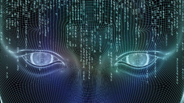
3. Brain implants.
4. Robotic hand that can recognize objects by Feel.
5. Upside-Down Rover to explore Europa.


Welcome to #18 Avatar Technology Digest. Again, get ready for exciting news on Technology, Medical Cybernetics and Artificial Intelligence. Thank you for watching us. You are welcome to Subscribe, follow us in social media, leave your comments and join the conversation. And here are the top stories of the last week.

1) A heart of foam could replace your own. Existing artificial hearts have multiple moving parts, which increases the chance of failure, but this new device is just a single piece of material. Researchers inspired by soft robots have built a pumping artificial heart that could one day replace the real deal.
The team of Bioengineers at Cornell University build their robots out of a solid, plastic foam, which naturally has an interconnected network of tubes to let air flow – just as our muscles are permeated by blood vessels. A solid coating of plastic seals everything inside like a skin.

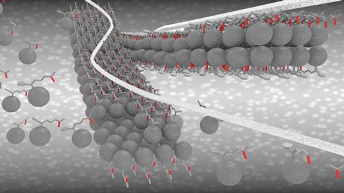
2) Researchers at QMUL have developed a way of assembling organic molecules into complex tubular tissue-like structures without the use of moulds or techniques like 3D printing. Self-assembling material can grow and change shape and one day could lead to artificial arteries.
The method uses solutions of peptide and protein molecules that, upon touching each other, self-assemble to form a dynamic tissue at the point at which they meet. As the material assembles itself it can be easily guided to grow into complex shapes.
This discovery could lead to the engineering of tissues like veins, arteries, or even the blood-brain barrier. The technique could also contribute to the creation of better implants, complex tissues, or more effective drug screening methods.

3) Neural Implant Enables Paralyzed ALS Patient to Type Six Words per Minute.
A massive collaboration of doctors and computer scientists gets one step closer to mind-controlled devices.
An eclectic team of researchers affiliated with BrainGate, a consortium of neuroscientists, engineers, computer scientists, and mathematicians, have published a study in Nature Medicine that profiles two subjects who control a cursor with their thoughts more deftly than previous systems allowed.
Earlier versions of the system allowed subjects to perform such tasks as drinking from a coffee thermos using a robotic arm, or playing simple games. The latest version brings finer control and ease of use. One participant was even able to type at a rate of six words a minute, using software originally developed to help people type type with eye movement.

4) Robots have many strong suits, but delicacy traditionally hasn’t been one of them. Rigid limbs and digits make it difficult for them to grasp, hold, and manipulate a range of everyday objects without dropping or crushing them. Now Soft robotic gripper can gently pick up and identify wide array of objects.
At a conference this month, researchers from Distributed Robotics Lab demonstrated a 3D-printed robotic hand made out of silicone rubber that can lift and handle objects as delicate as an egg and as thin as a compact disc.
Just as impressively, its three fingers have special sensors that can estimate the size and shape of an object accurately enough to identify it from a set of multiple items.

5) There’s a big ocean under the ice… NASA’s JPL team is working on a simple solution to get a sense of the deep ocean first: it’s working on the Buoyant Rover for Under-Ice Exploration. As you will see in the video, JPL tested it in choppy, methane-rich waters in Alaska.

TV Presenter: Olesya Yermakova @olesyayermakova.
Video: Vladimir Shlykov www.GetYourMedia.ru

Read more

For decades, researchers have been trying to build a computer that harnesses the enormous potential of quantum mechanics. Now engineers from the University of New South Wales (UNSW) in Australia have overcome the final hurdle, by creating a quantum logic gate in silicon — the same material that today’s computer chips are made from.

The newly developed device allows two quantum bits — or qubits — to communicate and perform calculations together, which is a crucial requirement for quantum computers. Even better, the researchers have also worked out how to scale the technology up to millions of qubits, which means they now have the ability to build the world’s first quantum processor chip and, eventually, the first silicon-based quantum computer.

Right now, regular computer chips store information as binary bits, which are either in a 0 or 1 state. This system works well, but it means that there’s a finite amount of data that can be processed. Qubits, on the other hand, can be in the state of 0, 1, or both at the same time, which gives quantum computers unprecedented processing power… if we can work out how to build them.

Read more

Following Moore’s law is getting harder and harder, especially as existing components reach their physical size limitations. Parts like silicon transistor contacts — the “valves” within a transistor that allow electrons to flow — simply can’t be shrunken any further. However, IBM announced a major engineering achievement on Thursday that could revolutionize how computers operate: they’ve figured out how to swap out the silicon transistor contacts for smaller, more efficient, carbon nanotubes.

The problem engineers are facing is that the smaller silicon transistor contacts get, the higher their electrical resistance becomes. There comes a point where the components simply get too small to conduct electrons efficiently. Silicon has reached that point. But that’s where the carbon nanotubes come in. These structures measure less than 10 nanometers in diameter — that’s less than half the size of today’s smallest silicon transistor contact. IBM actually had to devise a new means of attaching these tiny components. Known as an “end-bonded contact scheme” the 10 nm electrical leads are chemically bonded to the metal substructure. Replacing these contacts with carbon nanotubes won’t just allow for computers to crunch more data, faster. This breakthrough ensures that they’ll continue to shrink, following Moore’s Law, for several iterations beyond what silicon components are capable of.

“These chip innovations are necessary to meet the emerging demands of cloud computing, Internet of Things and Big Data systems,” Dario Gil, vice president of Science & Technology at IBM Research, said in a statement. “As technology nears the physical limits of silicon, new materials and circuit architectures must be ready to deliver the advanced technologies that will drive the Cognitive Computing era. This breakthrough shows that computer chips made of carbon nanotubes will be able to power systems of the future sooner than the industry expected.” The study will be formally published October 2nd, in the journal Science. This breakthrough follows a number of other recent minimization milestones including transistors that are only 3-atoms thick or constructed from a single atom.

Read more