Toggle light / dark theme

Just as the single-crystal silicon wafer forever changed the nature of electronics 60 years ago, a group of Cornell researchers is hoping its work with quantum dot solids – crystals made out of crystals – can help usher in a new era in electronics.

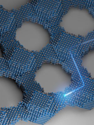
The multidisciplinary team, led by Tobias Hanrath, associate professor in the Robert Frederick Smith School of Chemical and Biomolecular Engineering, and graduate student Kevin Whitham, has fashioned two-dimensional superstructures out of single-crystal building blocks. Through directed assembly and attachment processes, the lead selenide quantum dots are synthesized into larger crystals, then fused together to form atomically coherent square superlattices.

The difference between these and previous crystalline structures is the atomic coherence of each 5-nanometer crystal (a nanometer is one-billionth of a meter). They’re not connected by a substance between each crystal – they’re connected directly to each other. The electrical properties of these superstructures potentially are superior to existing semiconductor quantum dots, with anticipated applications in solar cells and other electronic devices.
Read more

Years ago while I was still in college, I was able to experience what it was like working hands on in operations and logistics in retail. And, one of the most frustrating points was having to step away and log things on a desktop or try to locate your scanner to scan things in. I thought how wonderful it would be to be able to scan in receivables with my eyes and how much faster logistics would be. Although this article is from November; it highlights how VR really does improve things for companies, employees, and the quicker turn around time to customers.


A VR supply chain allows manufacturers to design and architect in 3-D, evaluate designs and make critical decisions about new products and customer buying decisions.

Read more

A new version of Atlas, designed to operate outdoors and inside buildings. It is electrically powered and hydraulically actuated. It uses sensors in its body and legs to balance and LIDAR and stereo sensors in its head to avoid obstacles, assess the terrain and help with navigation. This version of Atlas is about 5’ 9” tall (about a head shorter than the DRC Atlas) and weighs 180 lbs.

Read more

Graphene is too delicate to be produced commercially, but it seem that scientists have now stumbled upon the correct method of tuning it.

Graphene has many extraordinary properties. It is carbon, but it comes in the form of a two-dimensional, atomic thick, honeycomb lattice.

Remarkably, it is 100 times stronger than the strongest steel known to man, and is a very efficient conductor of heat and electricity. The possible applications for graphene-based electronics are myriad: they include better solar cells, OLEDs, batteries and supercapacitors, and they can also be used to make faster microchips that run on very little power.

Read more

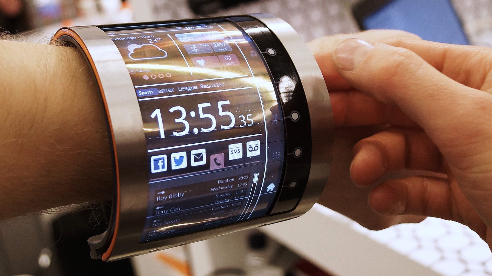
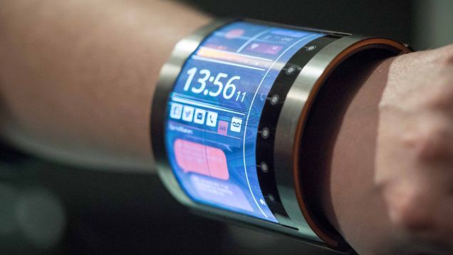
Sometimes, it seems like the tech world is inexorably bending towards a future full of curved devices. At MWC in Barcelona, we saw yet another prototype display, this time from English firm FlexEnable. Now, this isn’t a working device of any kind — it’s essentially just a screen running a demo — and neither is FlexEnable a consumer electronics company. But the firm says its technology is ready to go, and it’s apparently in talks with unnamed hardware partners who want to make this sort of device a reality. How long until we see fully-fledged wristbands like this on the market? Eighteen months is the optimistic guess from FlexEnable’s Paul Cain.

The prototype uses plastic transistors to achieve its flexibility, creating what the company calls OLCD (organic liquid crystal display) screens. FlexEnable says these can achieve the same resolutions as regular LCD using the same amount of power, but, of course, they have that added flexibility. These transistors can be wrapped around pretty much anything, and also have uses outside of display technology. FlexEnable was also showing off thin flexible fingerprint sensors, suggesting they could be wrapped around a door handle to add security without it being inconvenient to the user.

The prototype we saw at MWC was encased in a stiff metal frame, like a lot of flexible displays, and although OLCD can flex a little, it’s not the sort of material you can endlessly bend and crease. That, says, Cain, will have to wait for flexible OLED displays, a technology that is going to need more development. Still, we are seeing truly flexible OLED prototypes popping up here and there, such as this device from Queen’s University, which lets you flex a screen to flick through the pages of a digital book. The future bends ever closer.

Read more

Your smartwatch screen may soon be rather more impressive: This 4.7-inch organic LCD display is flexible enough to wrap right around a wrist.

Produced by FlexEnable from the UK, the screen squeezes a full-color organic LCD onto a sheet that measures just one hundredth of an inch thick, which makes it highly conformable. The company claims that it can easily run vivid colour and smooth video content, which is a sight better than most wearables.

It’s not the first flexible display, of course. LG already has an 18-inch OLED panel that has enough flexibility to roll into a tube that’s an inch across. But this concept—which, sadly, is all it is right now—is the first large, conformable OLCD designed for wearables that we’ve seen.

Read more

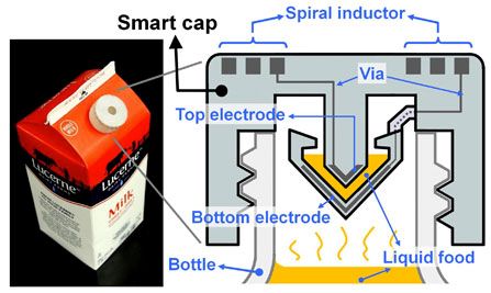
UC Berkeley engineers created a “smart cap” using 3-D-printed plastic with embedded electronics to wirelessly monitor the freshness of milk (credit: Photo and schematic by Sung-Yueh Wu)

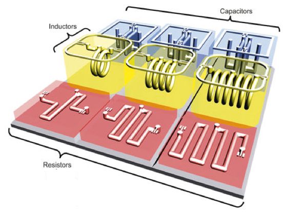
UC Berkeley engineers, in collaboration with colleagues at Taiwan’s National Chiao Tung University, have developed a 3D printing process for creating basic electronic components, such as resistors, inductors, capacitors, and integrated wireless electrical sensing systems.

As a test, they printed a wireless “smart cap” for a milk carton that detected signs of spoilage using embedded sensors.

Read more

Plasmonics, the study of how electrons behave in a metal under an electromagnetic field, requires the use of specialty coherent light sources as a basic tool. Optical interferometry can potentially become more important in biomedicine if only the technology could be made more compact, practical, and proven useful.

Toward that end researchers at Brown University have developed a way of using plasmonics techniques without using a coherent light source at all. This allows optical interferometry at the nanoscale and should lead to new types of biomedical sensors that can do rapid wide spectrum analysis for a variety of markers.

Here’s more details about the technology from Brown University:

Read more

Wireless Power Transmission Market reach $13.11 Billion by 2020. This is an area that I plan to keep a closer eye on especially since IEEE’s recent approved standards on sensors. I have a feeling that we could start seeing some major progress in this space.


DUBLIN, Jan. 27, 2016 /PR Newswire UK/ — Wireless Power Transmission Market (2015−2020) — Valued at $0.72 Billion in 2014 & Is Expected to Grow at a CAGR of 51.5%.

Read more

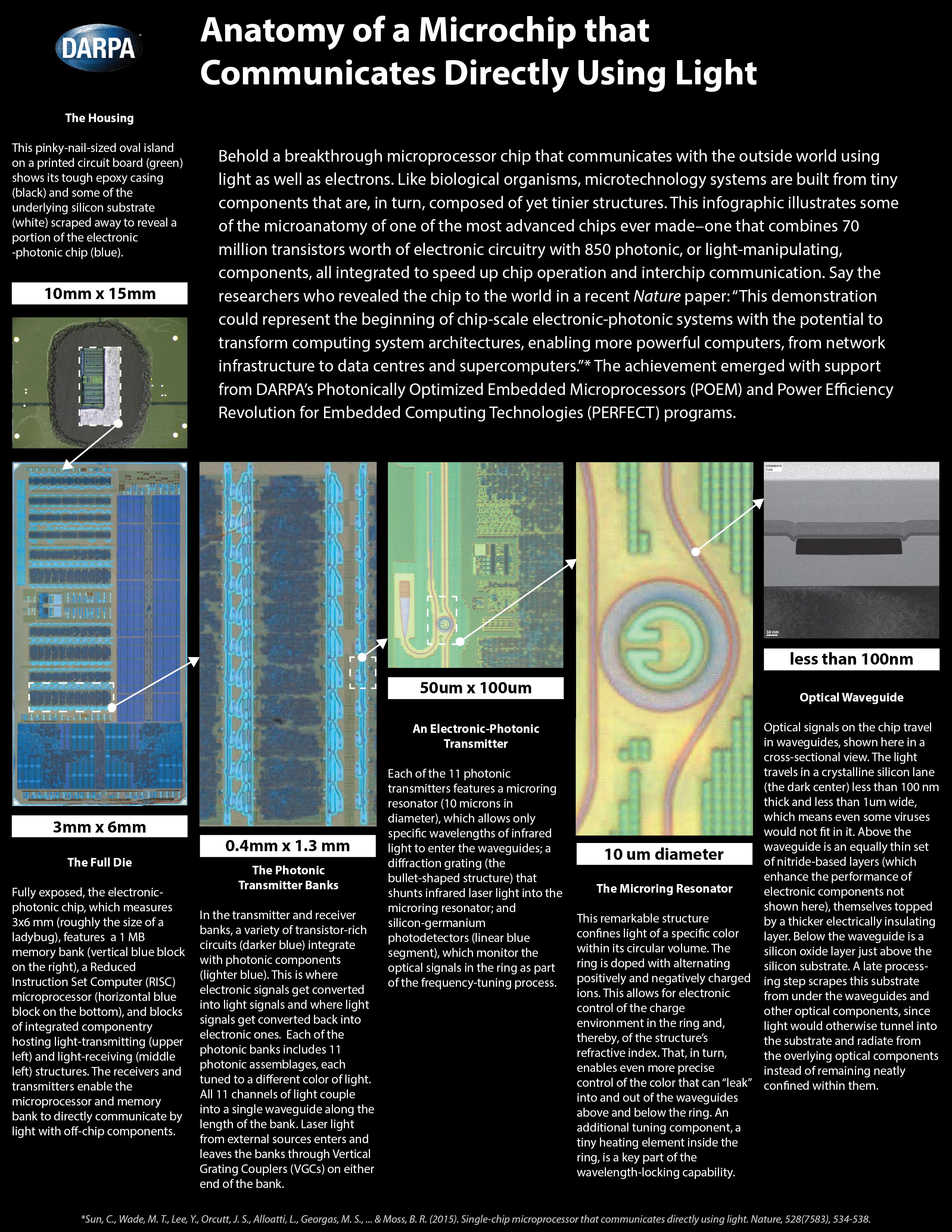
Integrated circuits traditionally have been a domain reserved for electrons, which course through exquisitely tiny transistors, wires and other microscopic structures where the digital calculations and data processing that underlie so much of modern technology unfold. Increasingly, however, chip designers have been acting on a long-ripening vision of enlisting photons instead of, or in tandem with, electrons in the operation of microprocessors. Photons, for one, can serve as fast-as-light carriers of information between chips, overcoming digital traffic jams that at times put the brakes on electrons. Recently, DARPA-funded scientists designed and crafted a breakthrough microprocessor that combines many of the best traits of electrons and photons on a single chip. The result is a remarkable and elegant hybrid microtechnology that boggles the mind for the intricate complexity of its sub-Lilliputian architecture. To appreciate the engineering acumen involved in the development of this chip and its tens of millions of resident electronic and photonic components, DARPA has produced an annotated, graphical tour of the new chip’s innards. Check it out, and lose yourself in a world of highways, toll gates and traffic circles populated by some of the physical world’s smallest commuters.

Infographic

Read more