Wicked nice — however, I cannot wait to see SamSung leverage Q-Dots (QD) for VR.
It’s Samsung’s best 4K UHD TV yet, and not just because it has stunning picture quality. It’s also the smartest, easiest-to-use TV we’ve seen in some time.

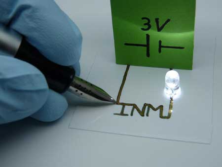
Research scientists at INM have combined the benefits of organic and inorganic electronic materials in a new type of hybrid inks. This allows electronic circuits to be applied to paper directly from a pen, for example.
The electronics of the future will be printed. Flexible circuits can be produced inexpensively on foil or paper using printing processes and permit futuristic designs with curved diodes or input elements. This requires printable electronic materials that can be printed and retain a high level of conductivity during usage in spite of their curved surfaces. Some tried and tested materials include organic, conductive polymers and nanoparticles made of conductive oxides (TCOs). Research scientists at INM – Leibniz-Institute for New Materials have now combined the benefits of organic and inorganic electronic materials in a new type of hybrid inks. This allows electronic circuits to be applied to paper directly from a pen, for example.
New hybrid inks permit printed, flexible electronics without sintering. (Image: INM)
Could this sensor technology revolutionize how auto and other navigation technology looks in the future?
The Defense Advanced Research Projects Agency (DARPA) has awarded HRL Laboratories $4.3 million to develop vibration- and shock-tolerant inertial sensor technology that enables future system accuracy needs without utilizing GPS.
While GPS provides sub-meter accuracy in optimal conditions, the signal is often lost or degraded due to natural interference or malicious jamming.
HRL Laboratories, based in Malibu, California, is a corporate research-and-development laboratory owned by The Boeing Company and General Motors specializing in research into sensors and materials, information and systems sciences, applied electromagnetics and microelectronics.
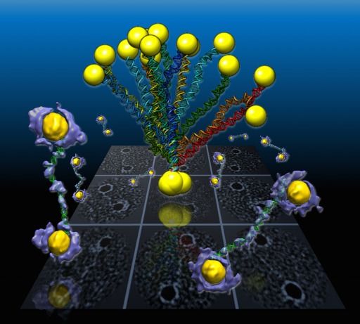
“DNA base pairing has been used for many years to direct the arrangement of inorganic nanocrystals into small groupings and arrays with tailored optical and electrical properties. The control of DNA-mediated assembly depends crucially on a better understanding of three-dimensional structure of DNA-nanocrystal-hybridized building blocks. Existing techniques do not allow for structural determination of these flexible and heterogeneous samples.”
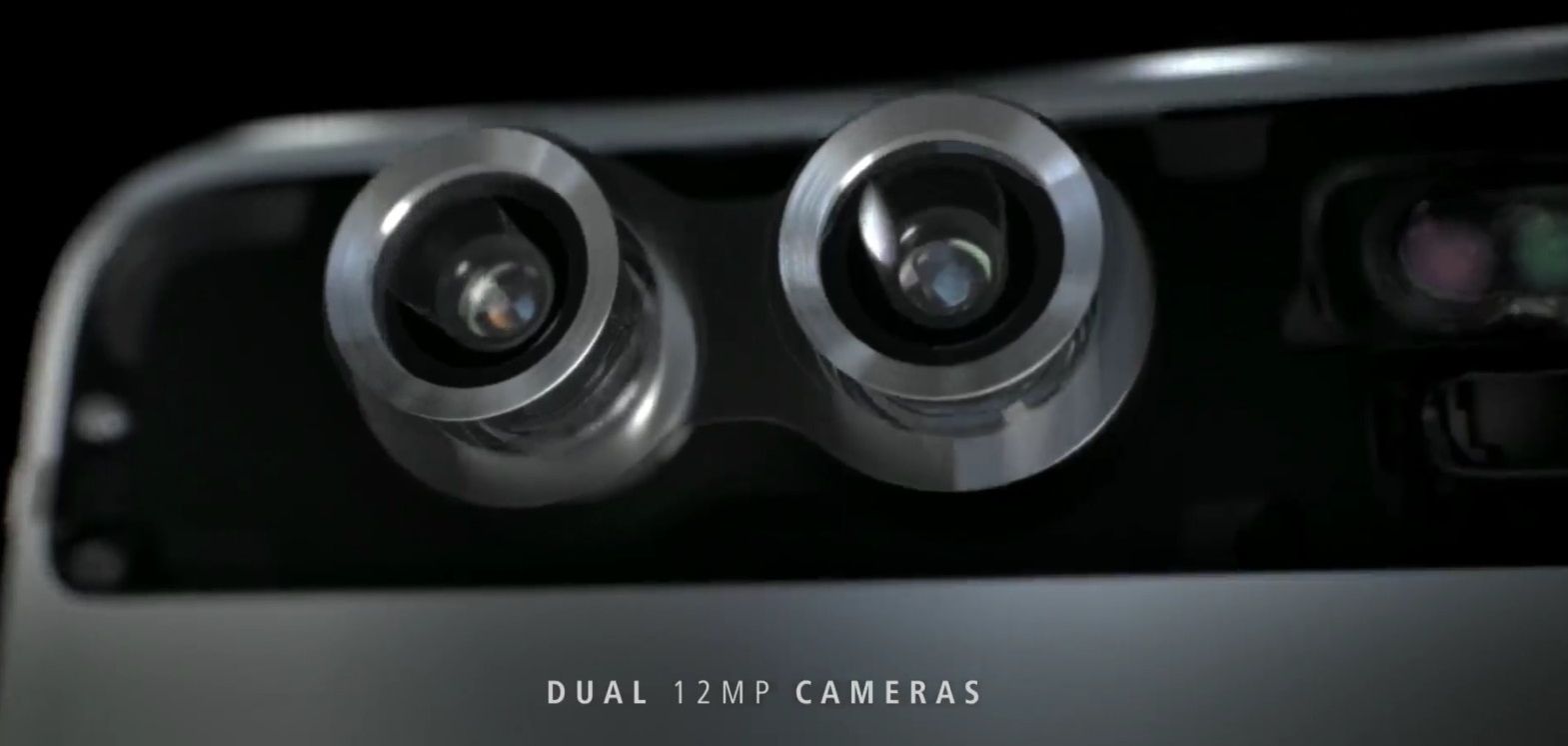
One of the biggest rumors surrounding the iPhone 7 is that Apple is adding a second camera module (at least on the Plus model), and it makes a lot more sense than you might realize.
After all, other manufacturers have already caught on. LG’s G5 comes with a ultra-wide angle lens, Huawei’s new P9 sports a dedicated black-and-white camera, and HTC beat everyone to the punch with the One M8’s depth-sensing camera a couple of years ago.
Our biggest ever edition of TNW Conference is fast approaching! Join 10,000 tech leaders this May in Amsterdam.
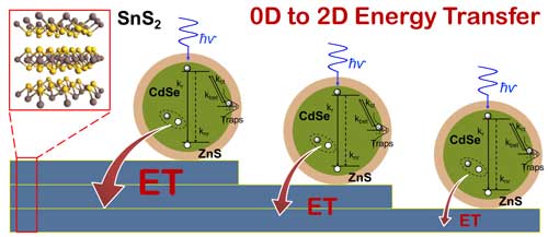
Improving light-sensing devices with Q-Dots.
Harnessing the power of the sun and creating light-harvesting or light-sensing devices requires a material that both absorbs light efficiently and converts the energy to highly mobile electrical current. Finding the ideal mix of properties in a single material is a challenge, so scientists have been experimenting with ways to combine different materials to create “hybrids” with enhanced features.
In two just-published papers, scientists from the U.S. Department of Energy’s Brookhaven National Laboratory, Stony Brook University, and the University of Nebraska describe one such approach that combines the excellent light-harvesting properties of quantum dots with the tunable electrical conductivity of a layered tin disulfide semiconductor. The hybrid material exhibited enhanced light-harvesting properties through the absorption of light by the quantum dots and their energy transfer to tin disulfide, both in laboratory tests and when incorporated into electronic devices. The research paves the way for using these materials in optoelectronic applications such as energy-harvesting photovoltaics, light sensors, and light emitting diodes (LEDs).
Single nanocrystal spectroscopy identifies the interaction between zero-dimensional CdSe/ZnS nano crystals (quantum dots) and two-dimensional layered tin disulfide as a non-radiative energy transfer, whose strength increases with increasing number of tin disulfide layers. Such hybrid materials could be used in optoelectronic devices such as photovoltaic solar cells, light sensors, and LEDs. (click on image to enlarge)
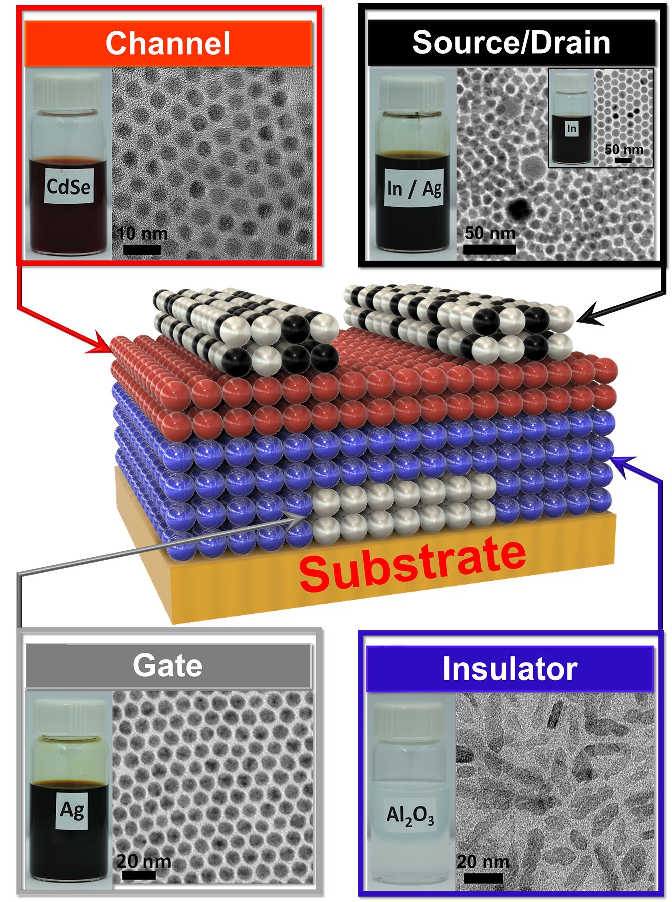
The transistor is the most fundamental building block of electronics, used to build circuits capable of amplifying electrical signals or switching them between the 0s and 1s at the heart of digital computation. Transistor fabrication is a highly complex process, however, requiring high-temperature, high-vacuum equipment.
Now, University of Pennsylvania engineers have shown a new approach for making these devices: sequentially depositing their components in the form of liquid nanocrystal “inks.”
Their new study, published in Science, opens the door for electrical components to be built into flexible or wearable applications, as the lower-temperature process is compatible with a wide array of materials and can be applied to larger areas.
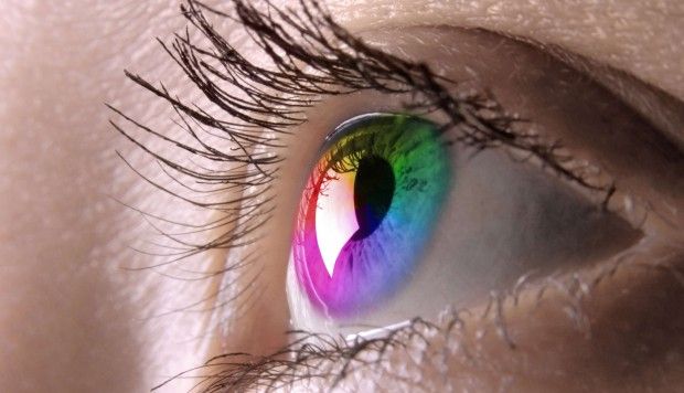
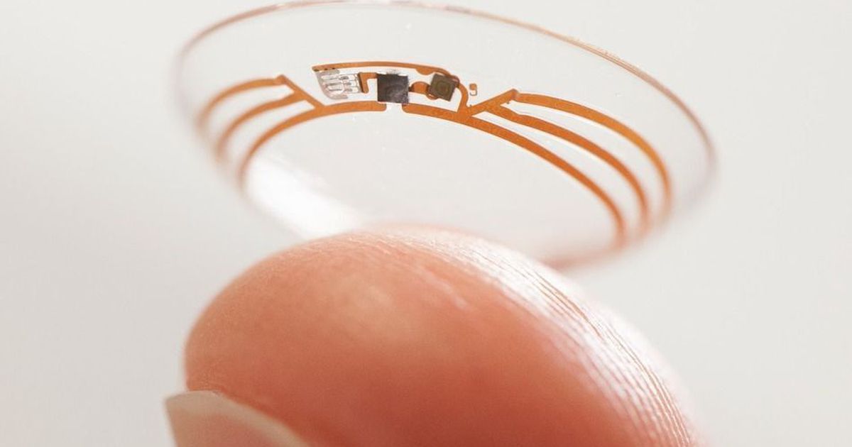
Samsung is exploring the development of a contact lens that can project images directly into the users’ eye, take photographs and connect wirelessly to a smartphone, a patent application has revealed.
The South Korean copyright authority has published a 29-page application made by the consumer electronics firm two years ago, reported the technology blog Sammobile, offering a rare insight into a science fiction vision of a future technology that could be closer than we think.
The lens could overlay internet-connected services directly into the user’s line of sight, in an example of what is known as augmented reality. It could also discreetly – even covertly – take photographs. The device would be controlled by eye movements or blinking, according to the patent, and it would connect with a smartphone.
