Toggle light / dark theme

If you’ve ever held a high-quality camera lens, the first thing you notice is the weight. Thanks to layers and layers of thick glass hunks inside, they end up being very heavy. However, thanks to research being done at Harvard on something called metalenses, one day those mgiant glass-filled lenses might be obsolete.

The curved surfaces on a glass lens focus incoming light onto a camera’s digital sensor. The more precise (and expensive) the lens is, the better the image it will produce.

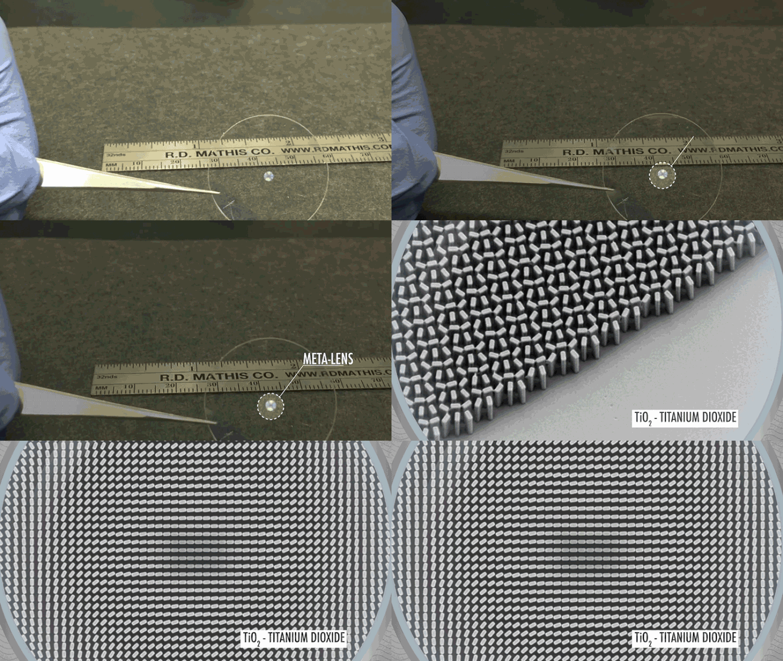
Metalenses work in a similar way, but they’re not made of precision-ground glass. Instead, a layer of transparent quartz is completely covered in a layer of tiny towers made from titanium dioxide. When arranged in specific patterns, those complex tower arrays can focus light exactly like a glass lens does. Except that these tiny metalenses end up being thinner than a human hair, and weigh almost nothing.
Read more

More energy efficient, high performance microprocessors on the way.


Abstract: Tiny high-performance lasers grown directly on silicon wafers solve a decades-old semiconductor industry challenge that, until now, has held back the integration of photonics with electronics on the silicon platform,

A group of scientists from Hong Kong University of Science and Technology; the University of California, Santa Barbara; Sandia National Laboratories and Harvard University were able to fabricate tiny lasers directly on silicon — a huge breakthrough for the semiconductor industry and well beyond.

For more than 30 years, the crystal lattice of silicon and of typical laser materials could not match up, making it impossible to integrate the two materials — until now.

Read more

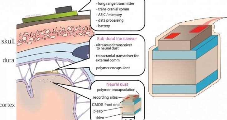
As the computation and communication circuits we build radically miniaturize (i.e. become so low power that 1 picoJoule is sufficient to bang out a bit of information over a wireless transceiver; become so small that 500 square microns of thinned CMOS can hold a reasonable sensor front-end and digital engine), the barrier to introducing these types of interfaces into organisms will get pretty low. Put another way, the rapid pace of computation and communication miniaturization is swiftly blurring the line between the technological base that created us and the technological based we’ve created. Michel Maharbiz, University of California, Berkeley, is giving an overview (june 16, 2016) of recent work in his lab that touches on this concern. Most of the talk will cover their ongoing exploration of the remote control of insects in free flight via implantable radio-equipped miniature neural stimulating systems.; recent results with neural interfaces and extreme miniaturization directions will be discussed. If time permits, he will show recent results building extremely small neural interfaces they call “neural dust,” work done in collaboration with the Carmena, Alon and Rabaey labs.

Radical miniaturization has created the ability to introduce a synthetic neural interface into a complex, multicellular organism, as exemplified by the creation of a “cyborg insect.”

“The rapid pace of computation and communication miniaturization is swiftly blurring the line between technological base we’ve created and the technological base that created us,” explained Dr. Maharbiz. “These combined trends of extreme miniaturization and advanced neural interfaces have enabled us to explore the remote control of insects in free flight via implantable radio-equipped miniature neural stimulating systems.”

Read more

When I 1st read this headline, I had to pause and ask myself “was the article’s author informed at all on QC?” especially given China’s own efforts much less D-Wave, Google, and University of Sydney. And, then I read the article and I still have to wonder if the author is on top of the emerging technologies such as BMI, graphene, QC, and other nanotechnology that are already being tested to go live in the next 7 to 10 years plus much of the content is very superficial at best. I am glad that the author did put the tid bit on Singularity as the endpoint state; however, that is pretty well known. Nonetheles, sharing to let you be the judge.


For decades, we relied on silicon as the semiconductor for our computer chips. But now, working at nanometer scales, it looks like physical limitations may end the current methods to include more and more processing power onto each individual chip.

Many companies are making billion-dollar investments to continue scaling down semiconductor technology. The pressures of big data and cloud computing are pushing the limits of the current semiconductor technology in terms of bandwidth, memory, processing speed, and device power consumption.

Today’s state-of-the-art silicon chips are engineered at the 22- and 14-nanometer scale. Research is underway to take that down to 10-nanometer scale in the next several years.

Read more

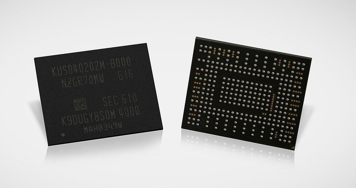
Storage in your laptop or smartphone is a compromise between volume, access speed and physical size. But, the industry’s competition to shrink them while boosting their specifications is fierce. A few months after shipping a 16TB solid-state drive, Samsung has announced a fast, efficient 512GB SSD that’s half the size of a postage stamp.

Samsung’s press release claims that the drive is the first mass-produced 512GB SSD with non-volatile memory express (NVMe), a host-controller interface with a streamlined register for speed, in a single package. Unlike other hard drives in multi-chip packages (MCP), Samsung’s new drive is organized in a ball grid array into a collected unit, making it simpler to fit in and connect to other parts in the device. This makes the drive ideal for the ultra-slim notebook PC market, where space and weight are at a premium.

A senior Samsung VP said in a press release that the tiny drive triples the performance of a typical SATA SSD. Its read/write speeds of up to 1,500MB/s and 900MB/s, respectively, mean you could transfer a 5GB HD video in 3 seconds. Samsung will start selling the drive in June in 512GB, 256GB and 128GB models.

Read more

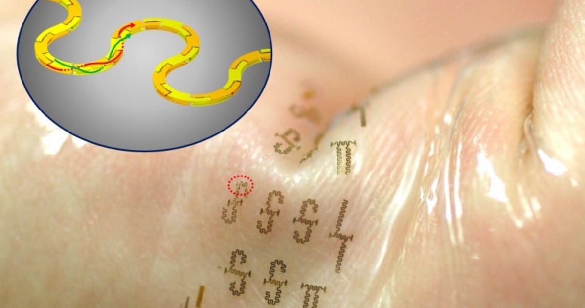
Make no mistake, today’s wearables are clever pieces of kit. But they can be bulky and restricted by the devices they must be tethered to. This has led engineers to create thinner and more powerful pieces of wearable technology that can be applied directly to the skin. Now, researchers at the University of Wisconsin-Madison, led by Zhenqiang “Jack” Ma, have developed “the world’s fastest stretchable, wearable integrated circuits,” that could let hospitals apply a temporary tattoo and remove the need for wires and clips.

With its snake-like shape, the new platform supports frequencies in the .3 gigahertz to 300 gigahertz range. This falls in what is set to become the 5G standard. For a mobile phone, 5G enables faster speeds and greater coverage, but with epidermal electronics, engineers have discussed the possibility that wearers could transmit their vitals to a doctor without having to leave their home.

While the idea isn’t unique, the integrated circuits created by Ma and his team have a much smaller footprint than those developed by other researchers. Earlier transmission lines can measure up to 640 micrometers (or .64 millimeters), but UW–Madison’s solution is just 25 micrometers (or .025 millimeters) thick. The Air Force Office of Scientific Research also supports Ma’s research, suggesting that his wearable breakthroughs may help pilots of the future.

Read more

New fundamental research by UT Dallas physicists may accelerate the drive toward more advanced electronics and more powerful computers.

The scientists are investigating materials called topological insulators, whose surface electrical properties are essentially the opposite of the properties inside.

“These materials are made of the same thing throughout, from the interior to the exterior,” said Dr. Fan Zhang, assistant professor of physics at UT Dallas. “But, the interior does not conduct electrons — it’s an insulator — while the electrons on the surface are free to move around. The surface is therefore a conductor, like a metal, but it is in fact more robust than a metal.”

Read more

The consumer marketplace is flooded with a lively assortment of smart wearable electronics that do everything from monitor vital signs, fitness or sun exposure to play music, charge other electronics or even purify the air around you — all wirelessly.

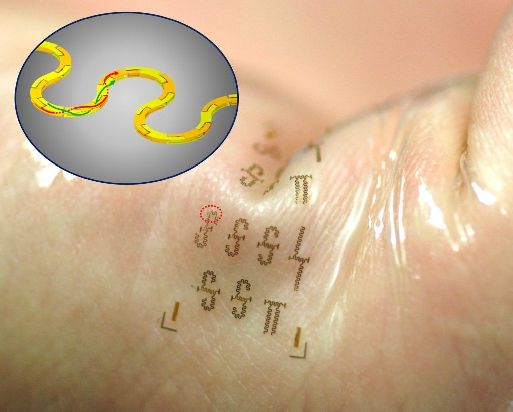
Now, a team of University of Wisconsin—Madison engineers has created the world’s fastest stretchable, wearable integrated circuits, an advance that could drive the Internet of Things and a much more connected, high-speed wireless world.

Led by Zhenqiang “Jack” Ma, the Lynn H. Matthias Professor in Engineering and Vilas Distinguished Achievement Professor in electrical and computer engineering at UW–Madison, the researchers published details of these powerful, highly efficient integrated circuits today, May 27, 2016, in the journal Advanced Functional Materials.

Read more