Toggle light / dark theme

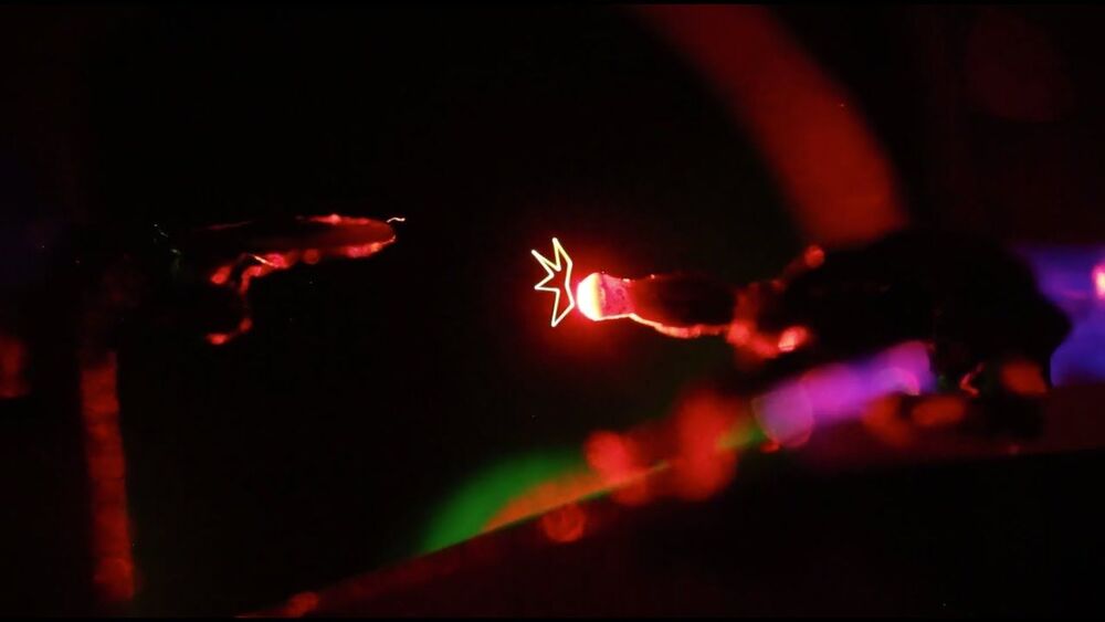
They may be tiny weapons, but Brigham Young University’s holography research group has figured out how to create lightsabers—green for Yoda and red for Darth Vader, naturally—with actual luminous beams rising from them.

Inspired by the displays of science fiction, the researchers have also engineered battles between equally small versions of the Starship Enterprise and a Klingon Battle Cruiser that incorporate photon torpedoes launching and striking the enemy vessel that you can see with the naked eye.

“What you’re seeing in the scenes we create is real; there is nothing computer generated about them,” said lead researcher Dan Smalley, a professor of electrical engineering at BYU. “This is not like the movies, where the lightsabers or the photon torpedoes never really existed in physical . These are real, and if you look at them from any angle, you will see them existing in that space.”

Widely used to monitor and map biological signals, to support and enhance physiological functions, and to treat diseases, implantable medical devices are transforming healthcare and improving the quality of life for millions of people. Researchers are increasingly interested in designing wireless, miniaturized implantable medical devices for in vivo and in situ physiological monitoring. These devices could be used to monitor physiological conditions, such as temperature, blood pressure, glucose, and respiration for both diagnostic and therapeutic procedures.

To date, conventional implanted electronics have been highly volume-inefficient—they generally require multiple chips, packaging, wires, and external transducers, and batteries are often needed for . A constant trend in electronics has been tighter integration of electronic components, often moving more and more functions onto the integrated circuit itself.

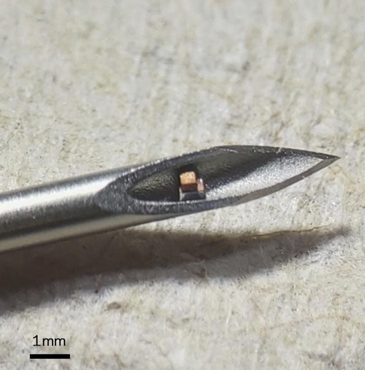
Researchers at Columbia Engineering report that they have built what they say is the world’s smallest single– system, consuming a total volume of less than 0.1 mm3. The system is as small as a dust mite and visible only under a microscope. In order to achieve this, the team used ultrasound to both power and communicate with the device wirelessly. The study was published online May 7 in Science Advances.

The findings could lead to faster, more secure memory storage, in the form of antiferromagnetic bits.

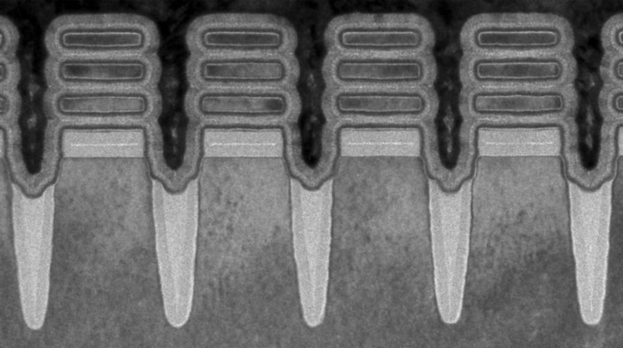
When you save an image to your smartphone, those data are written onto tiny transistors that are electrically switched on or off in a pattern of “bits” to represent and encode that image. Most transistors today are made from silicon, an element that scientists have managed to switch at ever-smaller scales, enabling billions of bits, and therefore large libraries of images and other files, to be packed onto a single memory chip.

But growing demand for data, and the means to store them, is driving scientists to search beyond silicon for materials that can push memory devices to higher densities, speeds, and security.

As the digital revolution has now become mainstream, quantum computing and quantum communication are rising in the consciousness of the field. The enhanced measurement technologies enabled by quantum phenomena, and the possibility of scientific progress using new methods, are of particular interest to researchers around the world.

Recently two researchers at Tampere University, Assistant Professor Robert Fickler and Doctoral Researcher Markus Hiekkamäki, demonstrated that two– interference can be controlled in a near-perfect way using the spatial shape of the photon. Their findings were recently published in the prestigious journal Physical Review Letters.

“Our report shows how a complex light-shaping method can be used to make two quanta of light interfere with each other in a novel and easily tuneable way,” explains Markus Hiekkamäki.

In 1884, Edwin Abbott wrote the novel Flatland: A Romance in Many Dimensions as a satire of Victorian hierarchy. He imagined a world that existed only in two dimensions, where the beings are 2D geometric figures. The physics of such a world is somewhat akin to that of modern 2D materials, such as graphene and transition metal dichalcogenides, which include tungsten disulfide (WS2), tungsten diselenide (WSe2), molybdenum disulfide (MoS2) and molybdenum diselenide (MoSe2).

Modern 2D materials consist of single-atom layers, where electrons can move in two dimensions but their motion in the third dimension is restricted. Due to this ‘squeeze’, 2D materials have enhanced optical and that show great promise as next-generation, ultrathin devices in the fields of energy, communications, imaging and quantum computing, among others.

Typically, for all these applications, the 2D materials are envisioned in flat-lying arrangements. Unfortunately, however, the strength of these materials is also their greatest weakness—they are extremely thin. This means that when they are illuminated, light can interact with them only over a tiny thickness, which limits their usefulness. To overcome this shortcoming, researchers are starting to look for new ways to fold the 2D materials into complex 3D shapes.

In 2001 at the Brookhaven National Laboratory in Upton, New York, a facility used for research in nuclear and high-energy physics, scientists experimenting with a subatomic particle called a muon encountered something unexpected.

To explain the fundamental physical forces at work in the universe and to predict the results of high-energy particle experiments like those conducted at Brookhaven, Fermilab in Illinois, and at CERN ’s Large Hadron Collider in Geneva, Switzerland, physicists rely on the decades-old theory called the Standard Model, which should explain the precise behavior of muons when they are fired through an intense magnetic field created in a superconducting magnetic storage ring. When the muon in the Brookhaven experiment reacted in a way that differed from their predictions, researchers realized they were on the brink of a discovery that could change science’s understanding of how the universe works.

Earlier this month, after a decades-long effort that involved building more powerful sensors and improving researchers’ capacity to process 120 terabytes of data (the equivalent of 16 million digital photographs every week), a team of scientists at Fermilab announced the first results of an experiment called Muon g-2 that suggests the Brookhaven find was no fluke and that science is on the brink of an unprecedented discovery.

Engineers at Duke University have developed the world’s first fully recyclable printed electronics. Their recycling process recovers nearly 100% of the materials used—and preserves most of their performance capabilities for reuse.

By demonstrating a crucial and relatively complex computer component—the transistor—created with three carbon-based inks, the researchers hope to inspire a new generation of recyclable electronics.

“Silicon-based computer components are probably never going away, and we don’t expect easily recyclable electronics like ours to replace the technology and devices that are already widely used,” said Aaron Franklin, the Addy Professor of Electrical and Computer Engineering at Duke. “But we hope that by creating new, fully recyclable, easily printed electronics and showing what they can do, that they might become widely used in future applications.”

John Martinis has done groundbreaking research on coherent superconducting devices since his PhD at the University of California, Berkeley, in 1985. These superconducting devices can be modeled as lumped-element electric circuits using Josephson junctions, capacitors and inductors as components. The fact that a superconducting phase across a Josephson junction can display coherent quantum behavior – even though it is a property of the wave function of an immense number of electrons – can be viewed as a fundamental discovery [1], kickstarting, in retrospect, the field of superconducting quantum computing.

John Martinis invented and developed the superconducting phase qubit, based on a current-biased Josephson junction, for the purpose of scalable multi-qubit quantum computing [2]. In 2002, he first demonstrated coherent Rabi oscillations and quantum measurement for such superconducting phase qubit [3]. He has had a longstanding interest in understanding the origin of noise in superconducting electric circuits as these sources of noise naturally limit qubit coherence. In particular, his understanding of noise sources such as dielectric loss, flux noise and the presence and dynamics of quasi-particles [4], by means of simple physical models, have been instrumental in the field. The effect and mitigation of quasi-particles and how they are affected by radiation and cosmic rays continues to be of high interest for the future of superconducting quantum devices [5, 6].

An important step showing his leadership and commitment to building a quantum computer came with his 2014 move, as a Professor at UCSB, to Google, where he gathered a large team of physicists and engineers to tackle the challenge of making a multi-qubit programmable processor. This team has excelled in its relentless focus on optimizing device performance by implementing successful engineering choices for qubit design, couplers and scalable I/O.