Toggle light / dark theme

Seagate has been working toward developing a dual-actuator hard drive, meaning that the drive will contain two sets of independently controlled read/write heads. Now, after several years, the company has released its first functional dual-actuator hard drive, the Mach.2. Currently, only enterprises can purchase and use this product, meaning that at least for now, end users will have to wait their turn.

So far, Seagate has reported the Mach.2’s sequential, sustained transfer rate as up to 524MBps—over double the rate of a fast but generic rust disk, closer to the capacity seen in SATA SSD. In fact, this increased carries over into input/output as well, featuring 304 IOPS read / 384 IOPS write and only 4.16 ms average latency. By contrast, normal hard drives usually run at 100/150 IOPS with about the same average latency.

Of course, all of that extra capacity requires additional power. Even while idle, the Mach.2 runs at 7.2 W, while Seagate’s standard Ironwolf line runs at 5 W while idle. That said, it is a bit easier to measure the power specs of Mach.2 than Ironwolf, as the former’s power use can be determined using several random input/output scenarios, as opposed to Ironwolf, whose power is gauged from its “average operating power,” a metric undefined by the Seagate data sheet reference.

The scale-free complexity associated with the biological system in general, and the neuron in particular, means that within each cell there is a veritable macromolecular brain, at least in terms of structural complexity, and perhaps to a certain degree functional complexity as well—a fractal hierarchy. This means that the extremely simplistic view of the synapse as a single digital bit is misrepresenting the reality of the situation—such as, if we were to utilize the parlance of the neurocomputational model, each ‘computational unit’ contains a veritable macromolecular brain within it. There is no computer or human technology yet equivalent to this.\.


A study published in the journal Science has upended 80 years of conventional wisdom in computational neuroscience that has modeled the neuron as a simple point-like node in a system, integrating signals and passing them along.

Combining self-assembly techniques from across scientific disciplines could allow us to precisely build any material structure.


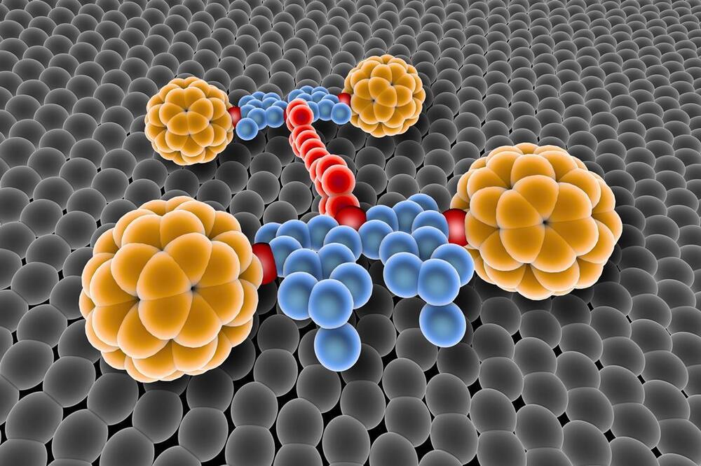
Nanocars are an impressive achievement – but nanoarchitectonics can unlock a far greater range of material structures.

In a lecture at the American Physical Society in 1959 titled ‘There’s Plenty of Room at the Bottom’, Richard Feynman argued that huge possibilities come from working in the world of molecules and atoms. He dreamed of ultra-small computers, cars running under a microscope, and medical machines working in our body.

These dreams are now coming true. In 2017, we had the first World Nanocar Race in Toulouse, France. Six teams from around the world manipulated nanometre-size cars to run on a metal surface under a scanning tunnelling microscope. A nanocar is 2 billion times smaller than a usual car, corresponding to the size difference between a rice grain and the Earth. Feynman only imagined cars 4000 times smaller than normal. However, few of the nanocars resembled cars, and none were powered by their own motors. There’s still plenty of room for improvement.

To meet soaring demand for lightning-quick mobile technology, each year tech giants create faster, more powerful devices with longer-lasting battery power than previous models.

A major reason companies like Apple and Samsung can miraculously pull this off year after year is because engineers and researchers around the world are designing increasingly power-efficient microchips that still deliver .

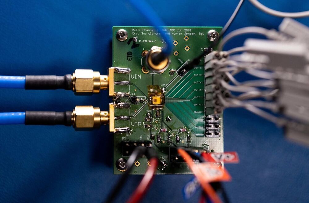
To that end, researchers led by a team at Brigham Young University have just built the world’s most power-efficient high-speed analog-to– (ADC) microchip. An ADC is a tiny piece of technology present in almost every electronic piece of equipment that converts analog signals (like a radio wave) to a digital signal.

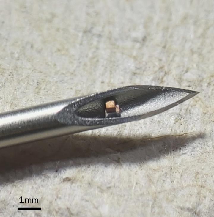
The continuing miniaturization of electronics is opening up some exciting possibilities when it comes to what we might place in our bodies to monitor and improve our health. Engineers at Columbia University have demonstrated an extreme version of this technology, developing the smallest single-chip system ever created, which could be implanted with a hypodermic needle to measure temperature inside the body, and possibly much more.

From ladybug-sized implants that track oxygen levels in deep body tissues to tiny “neural dust” sensors that monitor nerve signals in real time, scientists are making big steps when it comes to the functionality of tiny electronic devices. The implant developed by the Columbia Engineers breaks new ground as the world’s smallest single-chip system, which is a completely functional electronic circuit with a total volume of less than 0.1 mm3.

That makes it as small as a dust mite, and only visible under a microscope. The tiny chip required some outside-the-box thinking to make, particularly when it comes to the way it communicates and is powered.

Researchers at the Flatiron Institute’s Center for Computational Astrophysics published a paper last week that just might explain a mysterious gap in planet sizes beyond our solar system. Planets between 1.5 and 2 times Earth’s radius are strikingly rare. This new research suggests that the reason might be because planets slightly larger than this, called mini-Neptunes, lose their atmospheres over time, shrinking to become ‘super-Earths’ only slightly larger than our home planet. These changing planets only briefly have a radius the right size to fill the gap, quickly shrinking beyond it. The implication for planetary science is exciting, as it affirms that planets are not static objects, but evolving and dynamic worlds.

Exoplanet research is a very young field. As recently as 1992, no one had ever seen a planet beyond our solar system. Today, we’ve discovered more than 4700 of them, and that number is growing rapidly due to the efforts of dedicated planet-hunting space telescopes like Kepler (now defunct) and its successor, TESS. We’ve suddenly gained an enormous new sample size of planets to study, beyond the eight planets (sorry Pluto) that orbit around our sun.

Kepler, TESS, and other planet hunters have discovered brand new types of planets, like so-called ‘hot-Jupiters,’ large gas giants that orbit very close to their star. These were among the first exoplanets observed because their large size made them easy to find, and their small, fast orbital periods meant we could see them pass in front of their star more than once in a short period of time (some hot-Jupiters have a year that lasts only a few Earth days).

If you’ve been to your local beach, you may have noticed the wind tossing around litter such as an empty potato chip bag or a plastic straw. These plastics often make their way into the ocean, affecting not only marine life and the environment but also threatening food safety and human health.

Eventually, many of these plastics break down into microscopic sizes, making it hard for scientists to quantify and measure them. Researchers call these incredibly small fragments nanoplastics and microplastics because they are not visible to the naked eye. Now, in a multiorganizational effort led by the National Institute of Standards and Technology (NIST) and the European Commission’s Joint Research Centre (JRC), researchers are turning to a lower part of the food chain to solve this problem.

The researchers have developed a novel method that uses a filter-feeding marine species to collect these tiny plastics from ocean water. The team published its findings as a proof-of-principle study in the scientific journal Microplastics and Nanoplastics.

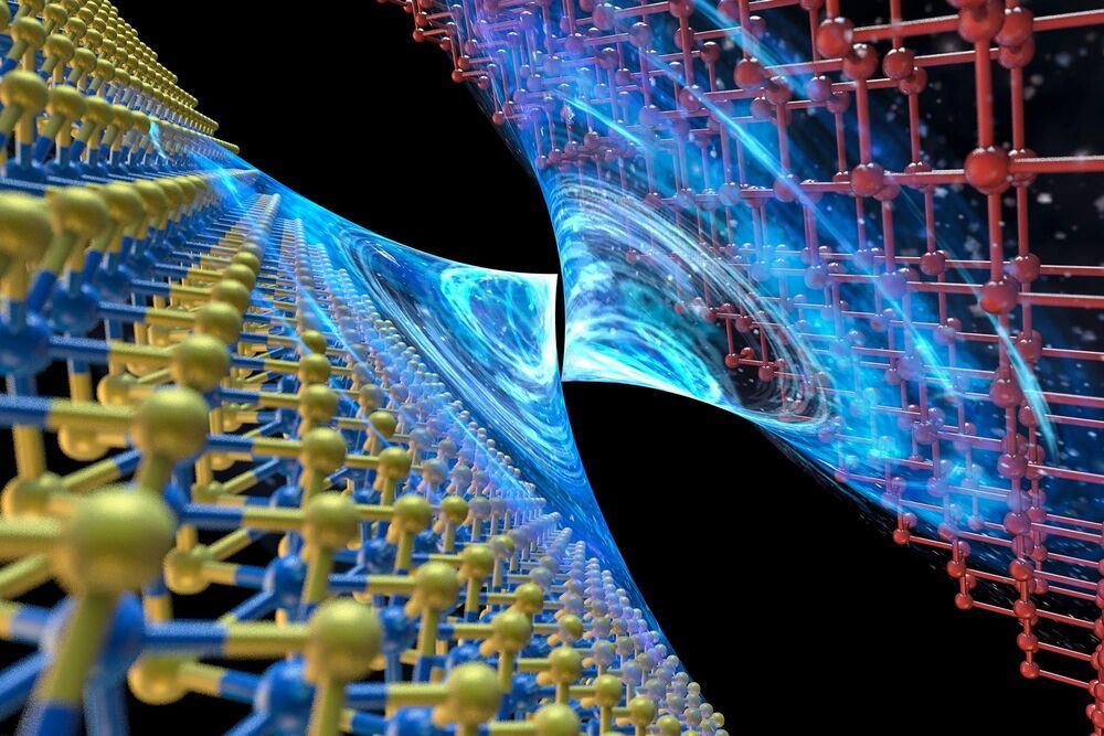
Atomically thin materials are a promising alternative to silicon-based transistors; now researchers can connect them more efficiently to other chip elements.

Moore’s Law, the famous prediction that the number of transistors that can be packed onto a microchip will double every couple of years, has been bumping into basic physical limits. These limits could bring decades of progress to a halt, unless new approaches are found.

One new direction being explored is the use of atomically thin materials instead of silicon as the basis for new transistors, but connecting those “2D” materials to other conventional electronic components has proved difficult.