Toggle light / dark theme

Using an ultrafast transmission electron microscope, researchers from the Technion – Israel Institute of Technology have, for the first time, recorded the propagation of combined sound and light waves in atomically thin materials.

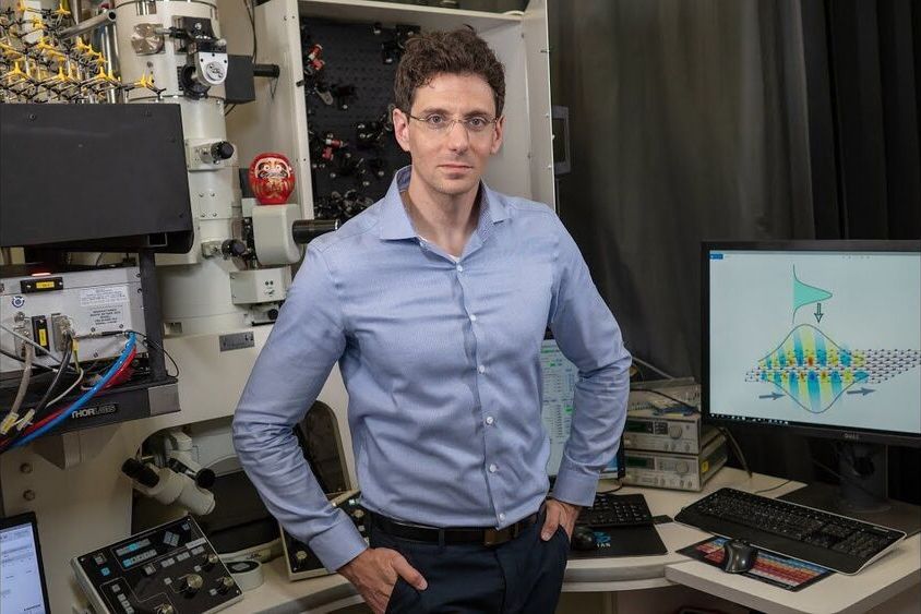
The experiments were performed in the Robert and Ruth Magid Electron Beam Quantum Dynamics Laboratory headed by Professor Ido Kaminer, of the Andrew and Erna Viterbi Faculty of Electrical & Computer Engineering and the Solid State Institute.

Single-layer materials, alternatively known as 2D materials, are in themselves novel materials, solids consisting of a single layer of atoms. Graphene, the first 2D material discovered, was isolated for the first time in 2004, an achievement that garnered the 2010 Nobel Prize. Now, for the first time, Technion scientists show how pulses of light move inside these materials. Their findings, “Spatiotemporal Imaging of 2D Polariton Wavepacket Dynamics Using Free Electrons,” were published in Science following great interest by many scientists.

With the established success of flexible computer screen displays, many users are wondering how display technology will advance next. So far, free-form displays have grown popular as a next-generation product that offers both portability and high-resolution visuals.

While this technology is still quite new, a wealth of research already exists into the stretchable displays that make up free form displays, products that can stretch into any direction like rubber.

On June 4, 2021, research at Samsung appeared in the well-known journal Science Advances discussing a technology that bypasses the limitations of stretchable devices. The associated experiment showed stable performance even when the was significantly elongated. As these products can already be used in existing semiconductor processes, Samsung researchers have high hopes about what this could mean for the commercialization and salability of stretchable devices.

Bill Gates isn’t going to use it to track you.


Your next doctor’s appointment could soon become much more informative thanks to new microchips the size of dust mites, only visible beneath a microscope.

Picture this: Your surgeon wants to continuously monitor your lungs prior to a procedure to ensure your respiratory system is strong enough to deal with anesthesia. So, a technician uses a hypodermic needle to inject a few small microchips into your body. Then, they use an ultrasound machine to communicate with the chips, which show your lungs are primed for the operation. Your subsequent surgery is a breeze.

This is a vision of the future with the world’s smallest single-chip system, a complete electronic circuit that technicians could one day inject directly into the body to monitor and diagnose certain health conditions.

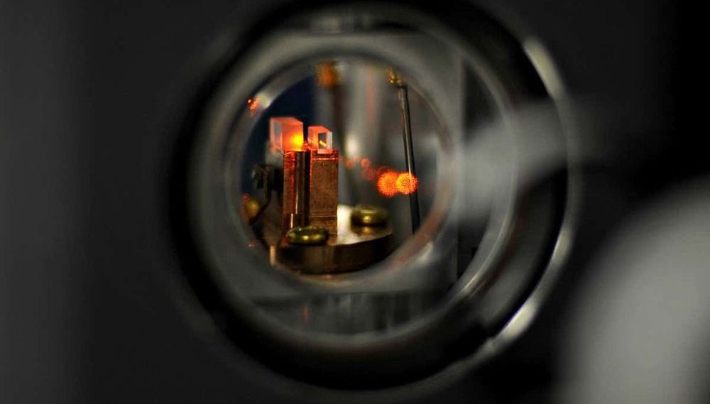
A secure quantum internet is one step closer thanks to a quantum memory made from a crystal, which could form a crucial part of a device able to transmit entangled photons over a distance of 5 kilometres. Crucially, it is entirely compatible with existing communication networks, making it suitable for real-world use.

There has long been a vision of a quantum version of the internet, which would allow quantum computers to communicate across long distances by exchanging particles of light called photons that have been linked together with quantum entanglement, allowing them to transmit quantum states.

The problem is that photons get lost when they are transmitted through long lengths of fibre-optic cable. For normal photons, this isn’t an issue, because networking equipment can simply measure and retransmit them after a certain distance, which is how normal fibre data connections work. But for entangled photons, any attempt to measure or amplify them changes their state.

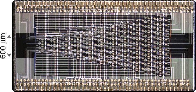
Just as microelectronics transformed the modern world through the creation of the integrated circuit, which is now at the heart of most electronic devices, quantum photonics needs an equivalent platform to fulfil its application potential. In this special focus issue of Nature Photonics, we report on the progress in making this a reality with the developments in integrated quantum photonics (IQP).

In a Review Article, Jianwei Wang and colleagues provide a general overview and introduction to IQP circuits and summarize the present development of quantum hardware based on IQP chips. They remark that the challenge for measurement-based quantum computation may shift from the need for deterministic gates to constructing a generic entangled cluster-state, on which any quantum computation could be mapped by a sequence of measurements.

IQP circuits are also a desirable platform for chip-based quantum communications. However, fully integrated chip-based quantum communication has not yet been realized, largely because of the integration difficulties between silicon wafers that feature optical waveguides and other passive components and light sources and photodetectors that are made from different semiconductors. Key components such as transmitters and receivers for quantum key distribution and quantum random number generators are instead individually fabricated.

Using an ultrafast transmission electron microscope, researchers from the Technion—Israel Institute of Technology have, for the first time, recorded the propagation of combined sound and light waves in atomically thin materials.

The experiments were performed in the Robert and Ruth Magid Electron Beam Quantum Dynamics Laboratory headed by Professor Ido Kaminer, of the Andrew and Erna Viterbi Faculty of Electrical & Computer Engineering and the Solid State Institute.

Single-layer materials, alternatively known as 2D materials, are in themselves novel materials, solids consisting of a single layer of atoms. Graphene, the first 2D material discovered, was isolated for the first time in 2004, an achievement that garnered the 2010 Nobel Prize. Now, for the first time, Technion scientists show how pulses of light move inside these materials. Their findings, “Spatiotemporal Imaging of 2D Polariton Wavepacket Dynamics Using Free Electrons,” were published in Science.

Google has helped create the most detailed map yet of the connections within the human brain. It reveals a staggering amount of detail, including patterns of connections between neurons, as well as what may be a new kind of neuron.

The brain map, which is freely available online, includes 50000 cells, all rendered in three dimensions. They are joined together by hundreds of millions of spidery tendrils, forming 130 million connections called synapses. The data set measures 1.4 petabytes, roughly 700 times the storage capacity of an average modern computer.

The data set is so large that the researchers haven’t studied it in detail, says Viren Jain at Google Research in Mountain View, California. He compares it to the human genome, which is still being explored 20 years after the first drafts were published.

Amazon Web Services (AMZN.O) said it will open data centers in Israel, with the announcement coming weeks after Israel signed a deal with AWS and Google for a more than $1 billion project to provide cloud services for its public sector and military.

In April, AWS and Google (GOOGL.O) won a tender for the four phase project known as “Nimbus”. read more

“Today, Amazon Web Services Inc, an Amazon.com company, announced it will open an infrastructure region in Israel in the first half of 2023”, AWS said in a statement on Friday.