Since today everybody is debating the question whether we live in a computer simulation, here is why I think Bostrom’s simulation argument is wrong:


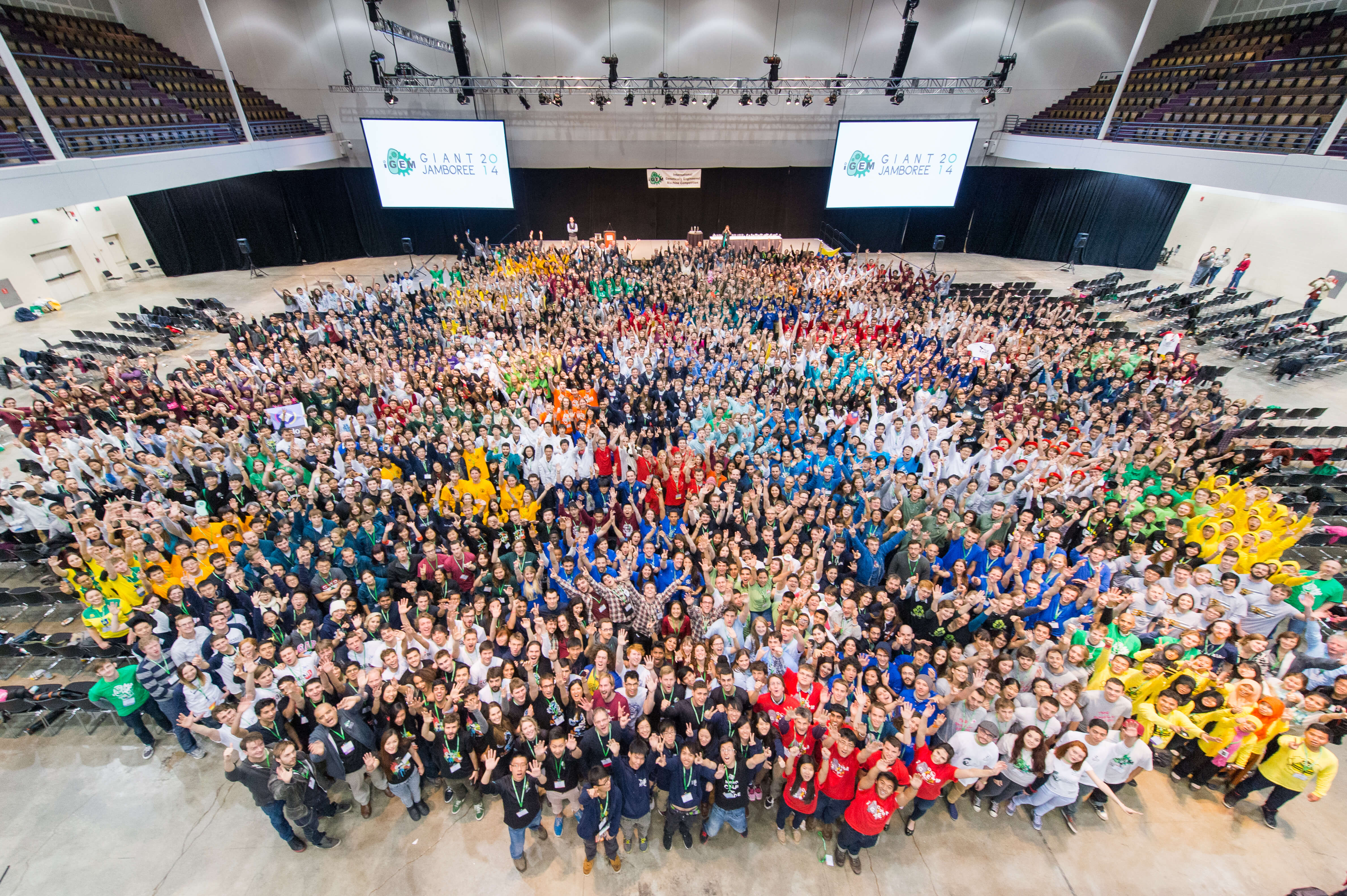
Agree; this is our future.
Almost ten years ago, Freeman Dyson ventured a wild forecast:
“I predict that the domestication of biotechnology will dominate our lives during the next fifty years at least as much as the domestication of computers has dominated our lives during the previous fifty years.”
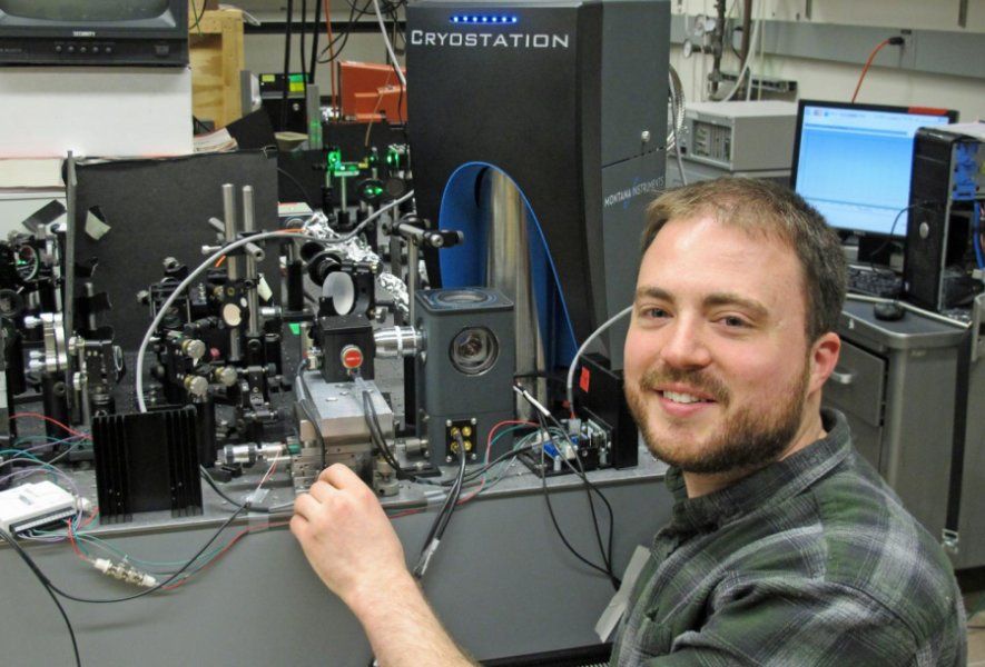
University of Oregon physicists have combined light and sound to control electron states in an atom-like system, providing a new tool in efforts to move toward quantum-computing systems.
The work was done on diamond topped with a layer of zinc oxide containing electrical conductors and performed at a temperature of 8 degrees Kelvin (−445.27 Fahrenheit, −265.15 Celsius) — just above absolute zero.
Using sound waves known as surface acoustic waves to change electron states could foster data transfer between quantum bits, the researcher said. The interaction of qubits, as is the case with binary bits in current computing, is seen as vital in building advanced systems.

Bots and artificial intelligence are all the rage right now. Whether it’s Siri or Cortana, computers are trying to take things off our plate and make life easier. Making life easier and more comfortable — and more luxurious — is what Bentley is about, too, and that’s why the company is imagining what the future of automotive luxury might be like.
One of those things, according to this mock-up image provided by Bentley, is a holographic butler that could appear in the car and help you out. Perhaps it would make restaurant recommendations and reservations, or you’d tell the digital Jeeves where you’re looking to go before your autonomous car takes over.
Bentley design director Stefan Sielaff said, according to The Mirror, that how these sorts of “yet-to-be-invented connectivity and technologies… are integrated into the cabin will become ever more important.” The holographic butler could put a more human face on the self-driving car, so just call out “Home, James!” and you’ll be on your way.
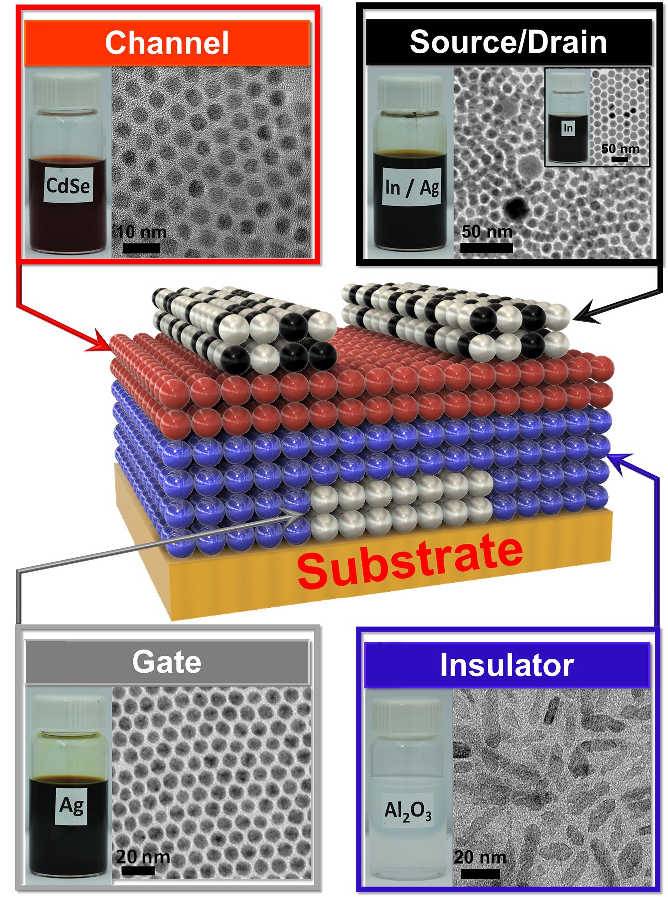
The transistor is the most fundamental building block of electronics, used to build circuits capable of amplifying electrical signals or switching them between the 0s and 1s at the heart of digital computation. Transistor fabrication is a highly complex process, however, requiring high-temperature, high-vacuum equipment.
Now, University of Pennsylvania engineers have shown a new approach for making these devices: sequentially depositing their components in the form of liquid nanocrystal “inks.”
Their new study, published in Science, opens the door for electrical components to be built into flexible or wearable applications, as the lower-temperature process is compatible with a wide array of materials and can be applied to larger areas.
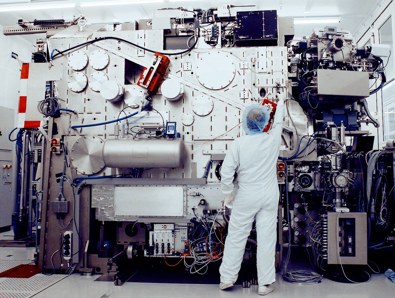
A new kind of nanoscale rectenna (half antenna and half rectifier) can convert solar and infrared into electricity, plus be tuned to nearly any other frequency as a detector.
Right now efficiency is only one percent, but professor Baratunde Cola and colleagues at the Georgia Institute of Technology (Georgia Tech, Atlanta) convincingly argue that they can achieve 40 percent broad spectrum efficiency (double that of silicon and more even than multi-junction gallium arsenide) at a one-tenth of the cost of conventional solar cells (and with an upper limit of 90 percent efficiency for single wavelength conversion).
It is well suited for mass production, according to Cola. It works by growing fields of carbon nanotubes vertically, the length of which roughly matches the wavelength of the energy source (one micron for solar), capping the carbon nanotubes with an insulating dielectric (aluminum oxide on the tethered end of the nanotube bundles), then growing a low-work function metal (calcium/aluminum) on the dielectric and voila–a rectenna with a two electron-volt potential that collects sunlight and converts it to direct current (DC).
“Our process uses three simple steps: grow a large array of nanotube bundles vertically; coat one end with dielectric; then deposit another layer of metal,” Cola told EE Times. “In effect we are using one end of the nanotube as a part of a super-fast metal-insulator-metal tunnel diode, making mass production potentially very inexpensive up to 10-times cheaper than crystalline silicon cells.”

Researchers at MIT’s Computer Science and Artificial Intelligence Laboratory (CSAIL) have developed a new 3D printing process that creates fully functional robots from the moment they come out of the printer.
MIT process of robot making is quite streamlined, as the robot’s solid and hydraulic parts are created in one step. CSAIL Director Daniela Rus, who oversaw the project, said that their approach of printable hydraulics is a step ahead in the rapid fabrication of functional machines.
The single-step process involves printing a small six-legged robot that crawls with the help of 12-hydraulic pumps embedded in its body. Working of the printer includes inkjet printer deposits drops of material quite small in size. The object is printed layer wise from bottom to the top. High-intensity UV light solidifies the materials that were used to create the object.
