Toggle light / dark theme

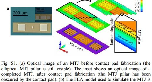
A new technique has been developed to implant high-performance magnetic memory chip on a flexible plastic surface without compromising performance.

It looks like a small piece of transparent film with tiny engravings on it, and is flexible enough to be bent into a tube. Yet, this piece of “smart” plastic demonstrates excellent performance in terms of data storage and processing capabilities. This novel invention, developed by researchers from the National University of Singapore (NUS), hails a breakthrough in the flexible electronics revolution, and brings researchers a step closer towards making flexible, wearable electronics a reality in the near future.

The technological advancement is achieved in collaboration with researchers from Yonsei University, Ghent University and Singapore’s Institute of Materials Research and Engineering. The research team has successfully embedded a powerful magnetic memory chip on a flexible plastic material, and this malleable memory chip will be a critical component for the design and development of flexible and lightweight devices. Such devices have great potential in applications such as automotive, healthcare electronics, industrial motor control and robotics, industrial power and energy management, as well as military and avionics systems.
Read more

Meet the world’s smallest hard drive.


Dutch scientists have developed a unique solution to deal with the data storage problem. By manipulating single atoms, researchers have created the world’s smallest hard drive capable of storing 1 kilobyte of data (8000 bits) in a space under 100 nanometers across. The technology means that all the books in the world could be stored on a device the size of a postage stamp.

In a study published Monday in the journal Nature Nanotechnology, scientists from the Technical University of Delft (TU Delft) said that they have created an atomic hard drive with a storage density that is 500 times greater than current hard drive technology.

Associate Professor at TU Delft and lead researcher Sander Otte and his team found that placing chlorine atoms on a copper surface created the perfect square grid. A hole appears in the grid when an atom is missing. Using a scanning tunneling microscope, scientists were able to move atoms around one by one and even drag individual atoms toward the hole.

Read more

More information on DARPA’s efforts in build new interface standards for modular design & practical circuit blocks.


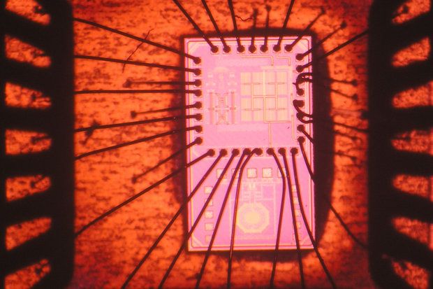
Is it possible to develop chip technology that combines the high-performance characteristics of ASICS with the speedy, low-cost features of printed circuit boards?

Scientists at the Defense Advanced Research Projects Agency this week said they were looking for information on how to build interface standards that would enable modular design and practical circuit blocks that could be reused to greatly shorten electronics development time and cost.

+More on Network World: DARPA: Researchers develop chip part that could double wireless frequency capacity +

One technique for addressing rising cost and complexity has been the use of a modular design flow that subdivides a system into functional circuit blocks, called IP blocks, DARPA stated. “IP block refers to intellectual property captured in a pre-designed functional circuit block. Examples of IP blocks include, but are not limited to, timing circuits, filters, waveform generators, embedded processors, data converters, amplifiers, fast Fourier transforms, serializer-deserializers and memory,” the agency stated.

Read more

Although BMI is nothing new; I never get tired of highlighting it.


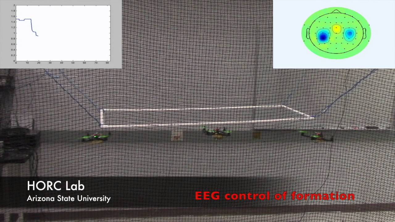
Now the group has come up with a way for one person to control multiple robots.

The system works using one controller who watches the drones, while his thoughts are read using a computer.

The controller wears a skull cap fitted with 128 electrodes wired to a computer. The device records electrical brain activity. If the controller moves a hand or thinks of something, certain areas light up.

Read more

Open the hood of just about any electronic gadget and you probably will find printed circuit boards (PCBs)—most often in a leaf-green color—studded with processing, memory, data-relaying, graphics, and other types of chips and components, all interconnected with a labyrinth of finely embossed wiring. By challenging the technology community to integrate the collective functions hosted by an entire PCB onto a device approaching the size of a single chip, DARPA’s newest program is making a bid to usher in a fresh dimension of technology miniaturization.

“We are trying to push the massive amount of integration you typically get on a printed circuit board down into an even more compact format,” said Dr. Daniel Green, manager of the new program, whose acronym, “CHIPS,” is itself a typographic feat of miniaturization; the program’s full name is the Common Heterogeneous Integration and Intellectual Property (IP) Reuse Strategies Program. “It’s not just a fun acronym,” Green said. “The program is all about devising a physical library of component chips, or chiplets, that we can assemble in a modular fashion.”

A primary driver of CHIPS is to develop a novel, industry-friendly architectural strategy for designing and building new generations of microsystems in which the time and energy it takes to move signals—that is, data—between chips is reduced by factors of tens or even hundreds. “This is increasingly important for the data-intensive processing that we have to do as the data sets we are dealing with get bigger and bigger,” Green said. Although the program does not specify applications, the new architectural strategy at the program’s heart could open new routes to computational efficiencies required for such feats as identifying objects and actions in real-time video feeds, real-time language translation, and coordinating motion on-the-fly among swarms of fast-moving unmanned aerial vehicles (UAVs).

Read more

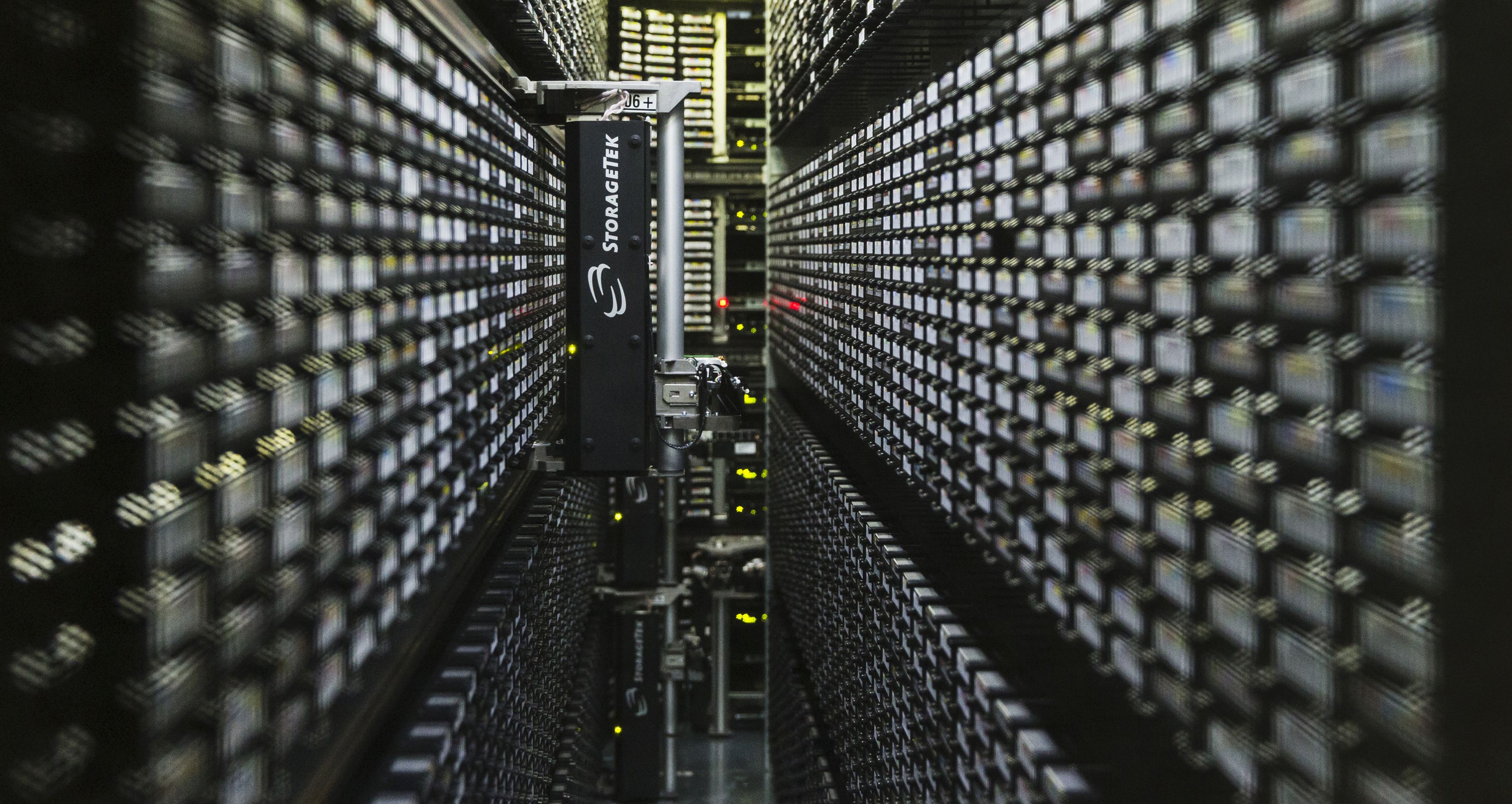
Every day, modern society creates more than a billion gigabytes of new data. To store all this data, it is increasingly important that each single bit occupies as little space as possible. A team of scientists at the Kavli Institute of Nanoscience at Delft University managed to bring this reduction to the ultimate limit: they built a memory of 1 kilobyte (8,000 bits), where each bit is represented by the position of one single chlorine atom.

“In theory, this storage density would allow all books ever created by humans to be written on a single post stamp”, says lead-scientist Sander Otte.

Read More on Delft University

Read more

Biowire.


Researchers led by microbiologist Derek Lovely say the wires, which rival the thinnest wires known to man, are produced from renewable, inexpensive feedstocks and avoid the harsh chemical processes typically used to produce nanoelectronic materials.

Lovley says, “New sources of electronic materials are needed to meet the increasing demand for making smaller, more powerful electronic devices in a sustainable way.” The ability to mass-produce such thin conductive wires with this sustainable technology has many potential applications in electronic devices, functioning not only as wires, but also transistors and capacitors. Proposed applications include biocompatible sensors, computing devices, and as components of solar panels.

This advance began a decade ago, when Lovley and colleagues discovered that Geobacter, a common soil microorganism, could produce “microbial nanowires,” electrically conductive protein filaments that help the microbe grow on the iron minerals abundant in soil. These microbial nanowires were conductive enough to meet the bacterium’s needs, but their conductivity was well below the conductivities of organic wires that chemists could synthesize.

Read more

Inspired by the large-scale sky surveys with which astronomers explore the cosmos, neuroscientists in Seattle, Washington, have spent four years systematically surveying the neural activity of the mouse visual cortex. The Allen Brain Observatory’s first data release, on 13 July, provides a publicly accessible data set of unprecedented size and scope, designed to help scientists to model and understand the human brain.

The project is part of an ambitious ten-year brain-research plan announced in 2012 by the Allen Institute for Brain Science. Designed to catalogue neurons and their electrical characteristics in minute detail, the initiative aims to enable new insights into how perception and cognition arise.

To compile the brain observatory’s first data set, researchers used a specialized microscope to record calcium waves that occur when neurons fire, sampling activity in 25 mice over 360 experimental sessions, while the animals viewed a battery of visual stimuli such as moving patterns of lines, images of natural scenes and short movies. The data set so far includes 18,000 cells in 4 areas of the visual cortex, making it one of the largest and most comprehensive of its kind. The set also includes information about each neuron’s location and its expression of certain genetic markers. At 30 terabytes, the raw data are too large to share easily, but users can download a more manageable processed data set, or explore it online.

Read more

About 5 years ago a friend of mine at Microsoft (Mitch S.) had a vision of making a new security model around drone swarms and a form of BMI technology. Glad to see the vision come true.


Scientists have discovered how to control multiple robotic drones using the human brain, an advance that can help develop swarms of search and rescue drones that are controlled just by thought.

A controller wears a skull cap outfitted with 128 electrodes wired to a computer. The device records electrical brain activity. If the controller moves a hand or thinks of something, certain areas light up. “I can see that activity from outside. Our goal is to decode that activity to control variables for the robots,” said Panagiotis Artemiadis, from the Arizona State University in the US. If the user is thinking about spreading the drones out, we know what part of the brain controls that thought, Artemiadis said.

A wireless system sends the thought to the robots. “We have a motion-capture system that knows where the quads are, and we change their distance,” he said. Up to four small robots, some of which fly, can be controlled with brain interfaces. To make them move, the controller watches on a monitor and thinks and pictures the drones performing various tasks.

Read more

3D print materials and products with superconducting properties is truly a breakthrough towards the mass production of various complex materials. I see this as a large step forward for 3D and placing things on an evolution track to even mass produce synthetic diamonds.


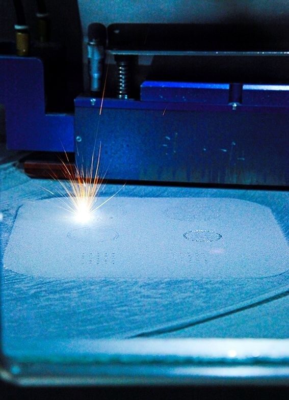
3D printing is revolutionizing many areas of manufacturing and science. In particular, 3D printing of metals has found novel applications in fields as diverse as customized medical implants, jet engine bearings and rapid prototyping for the automotive industry.

While many techniques can be used for 3D printing with metals, most rely on computer-controlled melting or sintering of a metal alloy powder by a laser or electron beam. The mechanical properties of parts produced by this method have been well studied, but not enough attention has focused on their electrical properties.

Now in a paper appearing this week on the cover of the journal Applied Physics Letters, a team of University of Melbourne and University of Western Australia researchers report creating a resonant microwave cavity that they 3D printed viaan aluminum-silicon alloy (Al-12Si). It exhibits superconductivity when cooled below the critical temperature of aluminum (1.2 Kelvin).

Read more