Toggle light / dark theme

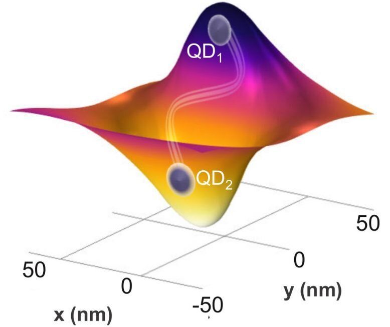
Researchers at CRANN and Trinity’s School of Physics have created an innovative new device that will emit single particles of light, or photons, from quantum dots that are the key to practical quantum computers, quantum communications, and other quantum devices.

The team has made a significant improvement on previous designs in photonic systems via their device, which allows for controllable, directional emission of single photons and which produces entangled states of pairs of .

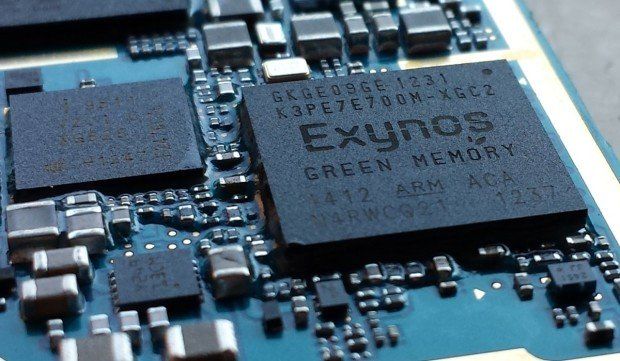
Samsung’s latest scientific breakthrough might change the very way we perceive semiconductors, largely on account of the fact it’s two-dimensional. Called amorphous boron nitride (a-BN), the substance in question is composed of but a single layer of atoms and characterized by an amorphous (liquid-like) molecule structure. It’s also the best 2D material for insulation ever synthetized, with Samsung hoping it will be able to utilize in production of revolutionary graphene wafers with unprecedentedly low level of electrical interference.

The discovery of a-BN is hardly Samsung’s first foray into 2D materials. The first and possibly most famous such substance — graphene — has been the subject of countless projects at the Korean conglomerate ever since it was first isolated in 2004. Following the 2016 Galaxy Note 7 fiasco, Samsung is believed to have doubled down on graphene R&D with the goal of eventually integrating the 2D material into its batteries, making them more stable, i.e. less prone to spontaneous combustions.

Making graphene batteries is no small feat, however, and it’s been a while since Samsung last made significant inroads on that front. Scalability remains a key issue, particularly in regards to mass-production costs. Graphene wafers, on the other hand, are expected to play a major role in the development and volume production of next-generation server memory modules, as well as DRAM and NAND memory chips.

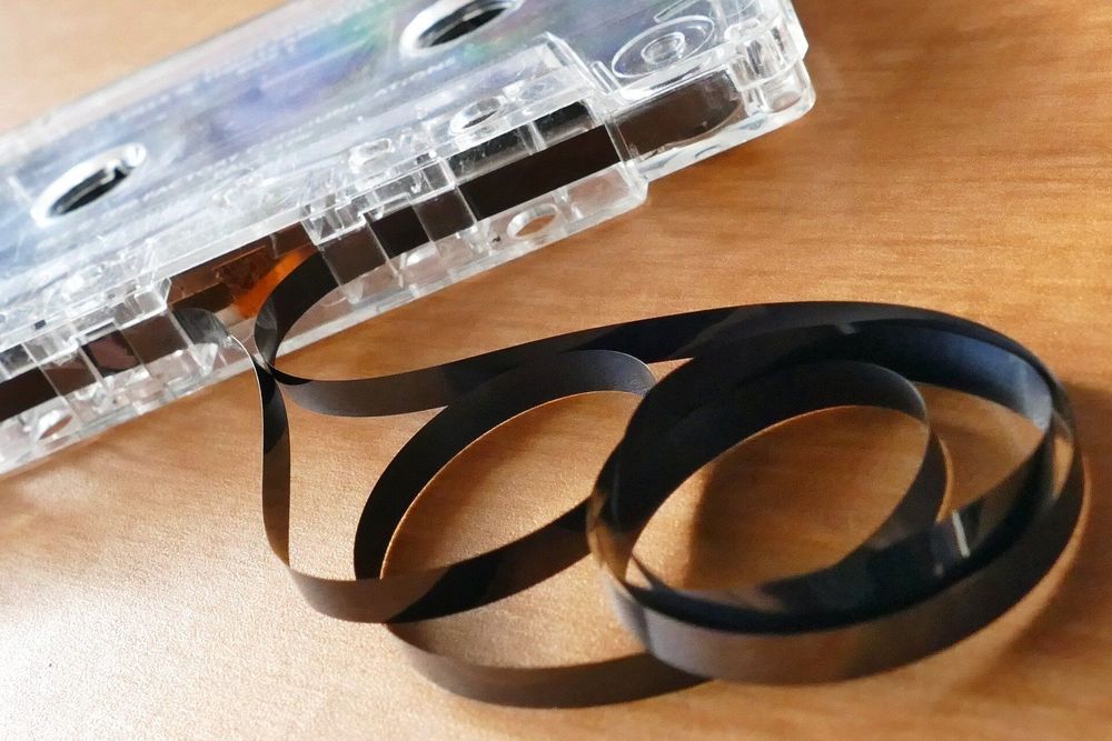
Fujifilm announced a technological breakthrough that will allow it to construct a massive 400 terabyte tape cartridge by the end of the decade.

Tape drives currently top out at about 12 terabytes of storage.

The Blocks and Files web site reported that Fujifilm says it can achieve the newer, greater capacities by switching from the standard Barium Ferrite (BaFe) tape coatings to Strontium Ferrite (SrFe).

Scientists at the University of Tsukuba use computer calculations to propose a new way to rearrange the carbon atoms in a diamond to make it even harder, which may be useful in industrial applications that rely on synthetic cutting diamonds.

Researchers at the University of Tsukuba used computer calculations to design a new carbon-based material even harder than diamond. This structure, dubbed “pentadiamond” by its creators, may be useful for replacing current synthetic diamonds in difficult cutting manufacturing tasks.

Diamonds, which are made entirely of carbon atoms arranged in a dense lattice, are famous for their unmatched hardness among known materials. However, carbon can form many other stable configurations, called allotropes. These include the familiar graphite in pencil lead, as well as nanomaterials such as carbon nanotubes. The mechanical properties, including hardness, of an allotrope depend mostly on the way its atoms bond with each other. In conventional diamonds, each carbon atom forms a covalent bond with four neighbors. Chemists call carbon atoms like this as having sp3 hybridization. In nanotubes and some other materials, each carbon forms three bonds, called sp2 hybridization.

The flight computers and avionics of NASA’s Space Launch System (SLS) rocket’s core stage for the Artemis I mission were powered on and have completed a thorough systems checkout. The test used Green Run software that was developed for the test and loaded in the flight computers for the first time. The SLS avionics power on and checkout was the second of eight tests in the Green Run test series at NASA’s Stennis Space Center near Bay St. Louis, Mississippi, where the core stage is installed in the B-2 Test Stand. The test steadily brought the core stage flight hardware, which controls the rocket’s first eight minutes of flight, to life for the first time. The three flight computers and avionics are located in the forward skirt, the top section of the 212-foot tall core stage, with more avionics distributed in the core’s intertank and engine section as shown in the right image. Engineers from NASA and Boeing, the core stage prime contractor, worked in control rooms as the avionic systems inside the Artemis I core stage, shown in the left image, were checked out. While this is the first time the Green Run software was used to control all the avionics in the flight core stage, engineers qualified the avionics and computers with earlier tests in the Systems Integration and Test Facility at NASA’s Marshall Space Flight Center in Huntsville, Alabama.

The core stage will provide more than 2 million pounds of thrust to help launch Artemis I, the first in a series of increasingly complex missions to the Moon through NASA’s Artemis program. NASA is working to land the first woman and next man on the Moon by 2024. SLS is part of NASA’s backbone for deep space exploration, along with NASA’s Orion spacecraft, the human landing system, and the Gateway in orbit around the Moon.

If you’ve got a mountain of digital data to store but don’t necessarily need to access it every day, tape cartridges are the way to go. Twelve terabytes of storage will set you back about $100 these days, but in the coming years, Fujifilm believes it can push the technology to 400TB capacities in a single cartridge.

NASA has released a stunning 61-minute time-lapse video that shows a decade in the life of the sun.

The video was created from images taken by NASA’s Solar Dynamics Observatory.

“From its orbit in space around Earth, SDO has gathered 425 million high-resolution images of the Sun, amassing 20 million gigabytes of data over the past 10 years,” explained NASA in a statement on its website. “This 10-year time lapse showcases photos taken at a wavelength of 17.1 nanometers, which is an extreme ultraviolet wavelength that shows the Sun’s outermost atmospheric layer – the corona.”

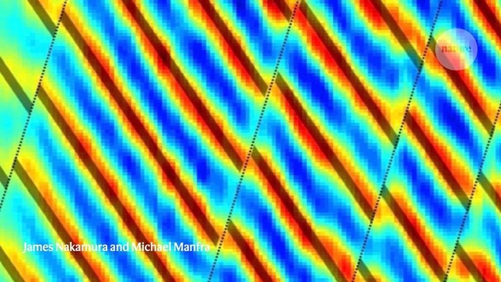
In a world’s first, researchers in France and the U.S. have performed a pioneering experiment demonstrating “hybrid” quantum networking. The approach, which unites two distinct methods of encoding information in particles of light called photons, could eventually allow for more capable and robust communications and computing.

Similar to how classical electronics can represent information as digital or analog signals, quantum systems can encode information as either discrete variables (DVs) in particles or continuous variables (CVs) in waves. Researchers have historically used one approach or the other—but not both—in any given system.

“DV and CV encoding have distinct advantages and drawbacks,” says Hugues de Riedmatten of the Institute of Photonic Sciences in Barcelona, who was not a part of the research. CV systems encode information in the varying intensity, or phasing, of light waves. They tend to be more efficient than DV approaches but are also more delicate, exhibiting stronger sensitivity to signal losses. Systems using DVs, which transmit information by the counting of photons, are harder to pair with conventional information technologies than CV techniques. They are also less error-prone and more fault-tolerant, however. Combining the two, de Riedmatten says, could offer “the best of both worlds.”