Toggle light / dark theme

Deep inside the electronic devices that proliferate in our world, from cell phones to solar cells, layer upon layer of almost unimaginably small transistors and delicate circuitry shuttle all-important electrons back and forth.

It is now possible to cram 6 million or more transistors into a single layer of these chips. Designers include layers of glassy between the electronics to insulate and protect these delicate components against the continual push and pull of heating and cooling that often causes them to fail.

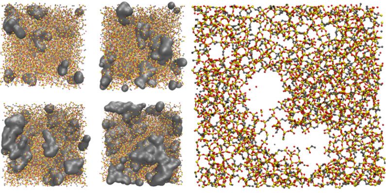
A paper published today in the journal Nature Materials reshapes our understanding of the materials in those important protective layers. In the study, Stanford’s Reinhold Dauskardt, a professor of materials science and engineering, and doctoral candidate Joseph Burg reveal that those respond very differently to compression than they do to the tension of bending and stretching. The findings overturn conventional understanding and could have a lasting impact on the structure and reliability of the myriad devices that people depend upon every day.

Read more

(credit: WEF)

The World Economic Forum’s annual list of this year’s breakthrough technologies, published today, includes “socially aware” openAI, grid-scale energy storage, perovskite solar cells, and other technologies with the potential to “transform industries, improve lives, and safeguard the planet.” The WEF’s specific interest is to “close gaps in investment and regulation.”

“Horizon scanning for emerging technologies is crucial to staying abreast of developments that can radically transform our world, enabling timely expert analysis in preparation for these disruptors. The global community needs to come together and agree on common principles if our society is to reap the benefits and hedge the risks of these technologies,” said Bernard Meyerson, PhD, Chief Innovation Officer of IBM and Chair of the WEF’s Meta-Council on Emerging Technologies.

The list also provides an opportunity to debate human, societal, economic or environmental risks and concerns that the technologies may pose — prior to widespread adoption.

Read more

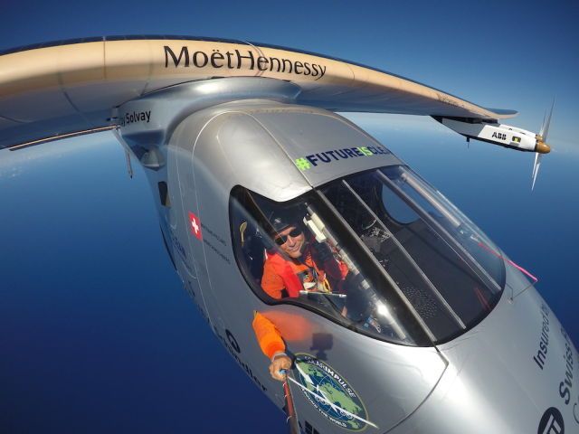
The flights take such a long time because Solar Impulse 2, as the name suggests, is completely powered by sunlight. The plane’s massive 72-metre wings (broader than a 747!) are covered in some 269.5 square metres of photovoltaic cells. During the day, the cells power four 14kW (17.4hp) electric motors and top-up four 41kWh lithium-ion batteries. During the evening, the motors are driven by the batteries. Max cruise speed when the sun is up is 49 knots (90km/h), and a rather languid 33 knots (60km/h) at night.

The solar cells don’t quite refill the batteries during the day, which means the plane can’t fly forever just yet. Max flight duration is somewhere around five to six days.

For power-saving reasons, the Solar Impulse 2 cockpit can only carry a single human, and is both unheated and unpressurised. The pilots do sleep while they’re up in the air, but usually just for 20 minutes at a time (the telemetry data for one flight showed 10 catnaps of 20 minutes over a 24-hour period). Now multiply those conditions by a continuous flight time of three or four days and you have some idea of the rigours that Piccard and Borschberg must go through.

Read more

Robert Dunleavy had just started his sophomore year at Lehigh University when he decided he wanted to take part in a research project. He sent an email to Bryan Berger, an assistant professor of chemical and biomolecular engineering, who invited Dunleavy to his lab.

Berger and his colleagues were conducting experiments on tiny semiconductor particles called quantum dots. The optical and electronic properties of QDs make them useful in lasers, light-emitting diodes (LEDs), medical imaging, solar cells, and other applications.

Dunleavy joined Berger’s group and began working with cadmium sulfide (CdS), one of the compounds from which QDs are fabricated. The group’s goal was to find a better way of producing CdS quantum dots, which are currently made with toxic chemicals in an expensive process that requires high pressure and temperature.

Read more

Nice.


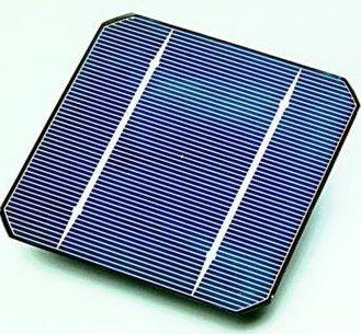
Scientists have designed new energy-carrying particles that improve the way electrons are transported and could be used to develop new types of solar cells and miniaturized optical circuitry.

The work of researchers at the University of California (UC) San Diego, MIT, and Harvard University has synthetically engineered particles called “topological plexcitons,” which can enhance a process known as exciton energy transfer, or EET.

It’s a problem scientists have been working on for years but it’s been tricky due to the short-ranged nature of EET, which is on the scale of only 10 nanometers, or 100 millionth of a meter, according to researchers. Moreover, the energy quickly dissipates as the excitons interact with different molecules.

Read more

Low-cost, low-dimensional nanoarchitectures provide optimal structures for charge collection in large-scale solar energy harvesting and conversion applications.

Photoelectrochemical water splitting, where irradiation of a photoelectrode in water produces hydrogen and oxygen, can be used for solar energy harvesting and conversion.1 The process potentially offers a clean, sustainable, and large-scale energy resource. Photoanodes used in the photoelectrochemical process are generally made from Earth-abundant oxide semiconductors, such as titanium dioxide, tungsten trioxide, and iron (III) oxide.2 Among these metal oxide semiconductors, tungsten trioxide is regarded as one of the best candidates because of its visible light-driven photocatalytic activity, its good charge transport properties, and its relative stability in aqueous electrolytes. However, the light absorption and charge collection efficiency of tungsten trioxide—especially within a bulk structure—still needs to be improved to realize practical photoelectrochemical applications.

Read more

Scientists at UC San Diego, MIT and Harvard University have engineered “topological plexcitons,” energy-carrying particles that could help make possible the design of new kinds of solar cells and miniaturized optical circuitry.

The researchers report their advance in an article published in the current issue of Nature Communications.

Within the Lilliputian world of solid state physics, light and matter interact in strange ways, exchanging energy back and forth between them.

Read more

The latest of the bionic leaf. A little over a year ago reseachers made an amazing discovery on cell circuitry leaves. Here is more news from Harvard on their research on bionic leaves.


Harvard scientists designed a new artificial photosynthesis system that turns sunlight into liquid fuel, and it is already effective enough for use in commercial applications.

Here’s an alternative source of energy many have never heard of— bionic leaves.

Scientists from Harvard University just made photosynthesis more efficient with what its creators are calling the “bionic leaf 2.0.” They’ve invented a new system that splits water molecules with solar energy and produces liquid fuels with hydrogen-eating bacteria.

Read more

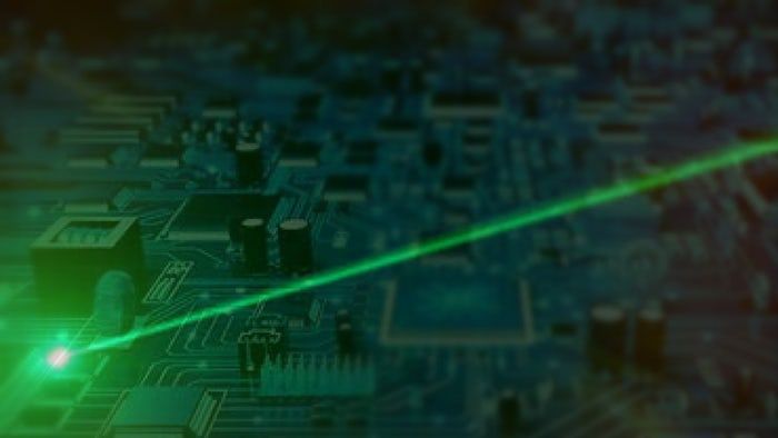
Silicon forms the basis of everything from solar cells to the integrated circuits at the heart of our modern electronic gadgets. However the laser, one of the most ubiquitous of all electronic devices today, has long been one component unable to be successfully replicated in this material. Now researchers have found a way to create microscopically-small lasers directly from silicon, unlocking the possibilities of direct integration of photonics on silicon and taking a significant step towards light-based computers.

Whilst there has been a range of microminiature lasers incorporated directly into silicon over the years, including melding germanium-tin lasers with a silicon substrate and using gallium-arsenide (GaAs) to grow laser nanowires, these methods have involved compromise. With the new method, though, an international team of researchers has integrated sub-wavelength cavities, the basic components of their minuscule lasers, directly onto the silicon itself.

To help achieve this, a team of collaborating scientists from Hong Kong University of Science and Technology, the University of California, Santa Barbara, Sandia National Laboratories and Harvard University, first had to find a way to refine silicon crystal lattices so that their inherent defects were reduced significantly enough to match the smooth properties found in GaAs substrate lasers. They did this by etching nano-patterns directly onto the silicon to confine the defects and ensure the necessary quantum confinement of electrons within quantum dots grown on this template.

Read more

Market forces often produce strange quirks in the economic system, like the one we’re seeing in Chile this year: the country is producing so much solar power that it’s being sold for… nothing at all.

While it’s incredibly encouraging to see so much expansion in the country’s renewable energy output, this huge amount of supply does actually cause problems for the companies looking to invest in solar energy.

Solar capacity on Chile’s central power grid (called SIC or Sistema Interconectado Central) has more than quadrupled over the past three years to 770 megawatts – good news for the environment and customers paying their electricity bills.

Read more