Toggle light / dark theme

Many consumers may have heard of blockchain technology, especially in relation to cryptocurrency. However, they may not be aware of its full potential and impact across industries. Blockchain has the potential to simplify and add greater security to data management, and since its inception, this technology has quietly been changing business processes.

To get further insights, we asked the members of Forbes Technology Council to share some ways blockchain has changed (or will soon change) business. Their best answers are below.


Photo:

Circa 2007


This chapter describes detection of explosives by terahertz Imaging ™. There has been an amplified interest in terahertz (THz) detection for imaging of covered weapons, explosives, chemical and biological agents. THz radiation is readily transmitted through most nonmetallic and nonpolar mediums. This process enables the THz systems to see through concealing barriers, which includes packaging, corrugated cardboard, clothing, shoes, book bags, and such others to find potentially dangerous materials concealed within. Apart from many materials of interest for security applications, which include explosives, chemical agents, and other such biological agents that have characteristic THz spectra which can be used for fingerprint testing and identify concealed materials. The Terahertz radiation poses either no or minimal health risk to either a suspect being scanned by a THz system or the system’s operator. As plastic explosives, fertilizer bombs, and chemical and biological agents increasingly become weapons of war and terrorism, and the trafficking of illegal drugs increasingly develops as a systemic threat, effective means for rapid detection, and an identification of these threats are required. One proposed solution for locating, detecting, and characterizing concealed threats is to use THz electromagnetic waves to spectroscopically detect and identify concealed materials through their characteristic transmission or reflectivity spectra in the range of 0.5–10 THz.

Circa 2019


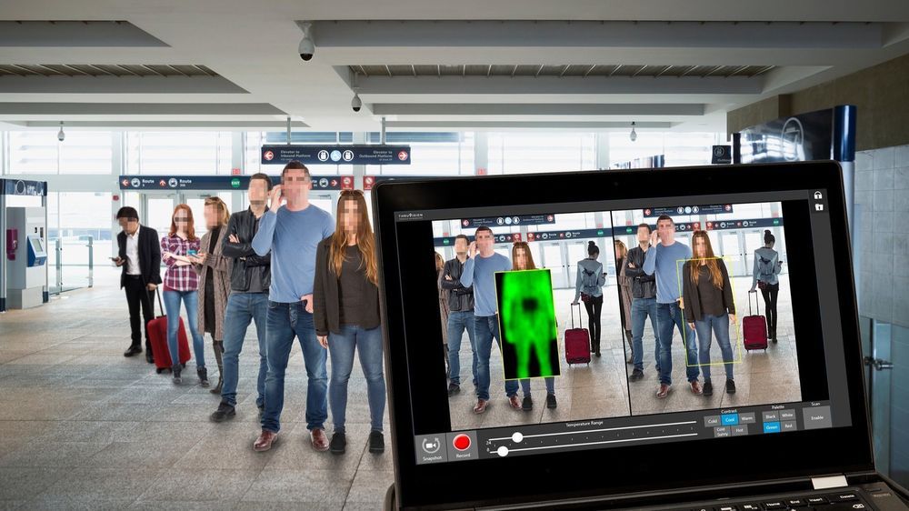
A full-body scanner that the Transportation Security Administration hopes can speed up airport security checkpoints must go back to the drawing board for software to protect the privacy of travelers being scanned.

The scanner, built by British firm Thruvision, was promoted as being able to simultaneously screen multiple airport passengers from a distance of up to 25 feet away. The TSA began trying out the device last year at an Arlington, Va., testing facility before planning to use it on a trial basis at U.S. airports.

But now the federal agency is requiring the scanner to add a “privacy filter” before the TSA can test the scanner “in a live environment,” according to a TSA document.

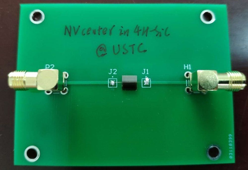
Decoherence is the bane of quantum technologies. In coherent systems, the phase of the wave functions representing the quantum states of particles in the system have definite relations between each other. This allows quantum devices to operate in a meaningful way that differs from classical devices. However, interacting with the world around us rapidly leads to decoherence, which makes it harder to exploit quantum effects for enhancing computation efficiency or communication security. Research has shown that quantum systems with impressively long coherence times are possible in diamond, but diamond is far from the favorite for manufacturers. Now, researchers at the University of Science and Technology in Hefei and Wuhan University in China have demonstrated SiC can boast some of the quantum merits of diamond with the additional advantage of optical control at the wavelengths used by the telecommunications industry.

The defects prized for quantum technologies are nitrogen-vacancy (NV) centers, in which a carbon atom in diamond is replaced by a nitrogen with a missing carbon at the neighboring crystal lattice site. What makes this kind of defect interesting for quantum technologies is that you can control its states with light and produce photon-spin entanglement with long coherence times, even at room temperature. The difficulties arise when trying to position the technology in the real world as opposed to the lab. The photon-spin interactions for NV centers in diamond need light at visible wavelengths—telecommunications wavelengths are much longer. In addition, these finely engineered devices need to be hacked out of one of the hardest (and most expensive) materials known to man, one that industry does not have established nanofabrication protocols for.

It turns out there are types of defects in SiC that might also be useful for quantum technologies. SiC is widely used in power electronics, so commercially viable avenues for producing SiC devices already exist. Over the past 10 years, vacancies and divacancies (where one or a pair of atoms in the lattice are absent) in SiC began to attract interest when researchers learned that they could also control their spin states with light at room temperature with long coherence times. The observation of NV centers in SiC really piqued interest, as these were optically active at the wavelengths used by the telecommunications industry as opposed to the shorter visible wavelengths needed to control the spin states of vacancies and divacancies in SiC.

As far back as 2015, the National Institute of Standards and Technology (NIST) began asking encryption experts to submit their candidate algorithms for testing against quantum computing’s expected capabilities — so this is an issue that has already been front of mind for security professionals and organizations. But even with an organization like NIST leading the way, working through all those algorithms to judge their suitability to the task will take time. Thankfully, others within the scientific community have also risen to the challenge and joined in the research.

It will take years for a consensus to coalesce around the most suitable algorithms. That’s similar to the amount of time it took ECC encryption to gain mainstream acceptance, which seems like a fair comparison. The good news is that such a timeframe still should leave the opportunity to arrive at — and widely deploy — quantum-resistant cryptography before quantum computers capable of sustaining the number of qubits necessary to seriously threaten RSA and ECC encryption become available to potential attackers.

The ongoing development of quantum-resistant encryption will be fascinating to watch, and security professionals will be sure to keep a close eye on which algorithms and encryption strategies ultimately prove most effective. The world of encryption is changing more quickly than ever, and it has never been more important for the organizations dependent on that encryption to ensure that their partners are staying ahead of the curve.

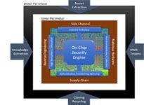
As Internet of Things (IoT) devices rapidly increase in popularity and deployment, economic attackers and nation-states alike are shifting their attention to the vulnerabilities of digital integrated circuit (IC) chips. Threats to IC chips are well known, and despite various measures designed to mitigate them, hardware developers have largely been slow to implement security solutions due to limited expertise, high cost and complexity, and lack of security-oriented design tools integrated with supporting semiconductor intellectual property (IP). Further, when unsecure circuits are used in critical systems, the lack of embedded countermeasures exposes them to exploitation. To address the growing threat this poses from an economic and national security perspective, DARPA developed the Automatic Implementation of Secure Silicon (AISS) program. AISS aims to automate the process of incorporating scalable defense mechanisms into chip designs, while allowing designers to explore chip economics versus security trade-offs based on the expected application and intent while maximizing designer productivity.

Today, DARPA is announcing the research teams selected to take on AISS’ technical challenges. Two teams of academic, commercial, and defense industry researchers and engineers will explore the development of a novel design tool and IP ecosystem – which includes tool vendors, chip developers, and IP licensors – allowing, eventually, defenses to be incorporated efficiently into chip designs. The expected AISS technologies could enable hardware developers to not only integrate the appropriate level of state-of-the-art security based on the target application, but also balance security with economic considerations like power consumption, die area, and performance.

“The ultimate goal of the AISS program is to accelerate the timeline from architecture to security-hardened RTL from one year, to one week – and to do so at a substantially reduced cost,” said the DARPA program manager leading AISS, Mr. Serge Leef.

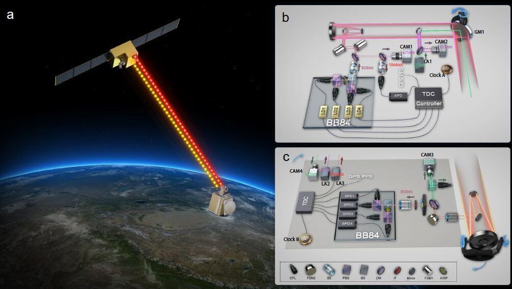
Researchers at the University of Science and Technology of China have recently introduced a new satellite-based quantum-secure time transfer (QSTT) protocol that could enable more secure communications between different satellites or other technology in space. Their protocol, presented in a paper published in Nature Physics, is based on two-way quantum key distribution in free space, a technique to encrypt communications between different devices.

“Our main idea was to realize quantum-secure time transfer in order to resolve the in practical time–frequency transfer,” Feihu Xu, one of the researchers who carried out the study, told Phys.org.

Quantum key distribution (QKD) is a technique to achieve secure communication that utilize based on the laws of quantum mechanics. Quantum protocols can generate secret security keys based on , enabling more secure data transfer between different devices by spotting attackers who are trying to intercept communications.

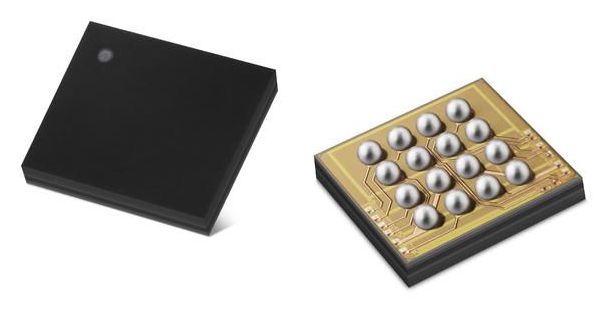
Samsung has launched a new secure element (SE) chip to protect private and sensitive data on mobile devices, the company said on Tuesday.

The chip, dubbed S3FV9RR, will be offered as a standalone turnkey with security software, Samsung said.

Common Criteria, which certifies the security level of IT products from EAL0 to EAL7 with seven being the most secure, gave the security chip a Common Criteria Evaluation Assurance Level (CC EAL) 6+ certification.

April 2020


Field programmable gate arrays, FPGAs for short, are flexibly programmable computer chips that are considered very secure components in many applications. In a joint research project, scientists from the Horst Görtz Institute for IT Security at Ruhr-Universität Bochum and from Max Planck Institute for Security and Privacy have now discovered that a critical vulnerability is hidden in these chips. They called the security bug “Starbleed.” Attackers can gain complete control over the chips and their functionalities via the vulnerability. Since the bug is integrated into the hardware, the security risk can only be removed by replacing the chips. The manufacturer of the FPGAs has been informed by the researchers and has already reacted.

The researchers will present the results of their work at the 29th Usenix Security Symposium to be held in August 2020 in Boston, Massachusetts, U.S… The has been available for download on the Usenix website since April 15, 2020.

Focus on the bitstream

FPGA chips can be found in many safety-critical applications today, from cloud data centers and mobile phone base stations to encrypted USB-sticks and industrial control systems. Their decisive advantage lies in their reprogrammability compared to conventional hardware chips with their fixed functionalities.