Toggle light / dark theme

Amazon Web Services (AWS) is partnering with the Hebrew University of Jerusalem for a new quantum computing initiative as part of the company’s efforts, launched in 2019, to explore this area of research. These include a cloud-based quantum computing service Amazon Braket to accelerate research and discovery, the Amazon Quantum Solutions Lab to help businesses explore quantum applications, and the AWS Center for Quantum Computing research and development organization.

AWS’ latest collaboration with Hebrew University will fund a team of researchers from the academic institution’s Quantum Information Science Center (QISC), founded in 2013, and the Racah Institute of Physics to advance the understanding of quantum gates – fundamental building blocks of quantum computers, the parties said in a statement on Monday. The collaboration is the first between AWS and any Israeli academic institution in the field.

The university’s Professor Alex Retzker, a researcher of quantum technologies, will lead the research group as part of his role as a Principal Research Scientist at AWS.

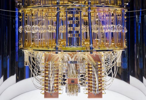
Yesterday Nvidia officially dipped a toe into quantum computing with the launch of cuQuantum SDK, a development platform for simulating quantum circuits on GPU-accelerated systems. As Nvidia CEO Jensen Huang emphasized in his keynote, Nvidia doesn’t plan to build quantum computers, but thinks GPU-accelerated platforms are the best systems for quantum circuit and algorithm development and testing.

As a proof point, Nvidia reported it collaborated with Caltech to develop “a state-of-the-art quantum circuit simulator with cuQuantum running on NVIDIA A100 Tensor Core GPUs. It generated a sample from a full-circuit simulation of the Google Sycamore circuit in 9.3 minutes on Selene, a task that 18 months ago experts thought would take days using millions of CPU cores.”

Majorana modes are, however, notoriously elusive. In part, this is because it is hard to create the conditions required to generate them in an experimental setting. Many theoretical proposals have predicted MZMs should be present in quasi-2D materials, which consist of a small number of 2D layers stacked on top of each other. However, all previous proposals required heterostructures – that is, structures where the stacked layers have differing material composition and structure. Practically, these heterostructures are difficult if not downright impossible to grow.

To make matters worse, Majorana modes can only be observed indirectly. Like detectives trying to catch a culprit with only circumstantial evidence, physicists have a hard time ruling out alternative explanations for the phenomena they observe. This has led to high-profile premature claims of Majorana discovery, including Microsoft Quantum Lab’s recent retraction of a Nature paper in which they purported to observe MZMs in nanowires.

In their new work, Zhang and his coauthor show that Majorana modes should be present in a much simpler setting: thin films of an iron-based superconducting material. Like previous proposals, the system they study is quasi-2D, but crucially all layers are of the same kind. The iron-based thin films naturally accommodate Majorana fermions that are helical – left or right-handed – and move along the edges of the system in their preferred direction. This is due to a special “time-reversal” symmetry, wherein interchanging the left-moving and right-moving quasiparticles makes it look like time is propagating backwards in the system.

Physics World


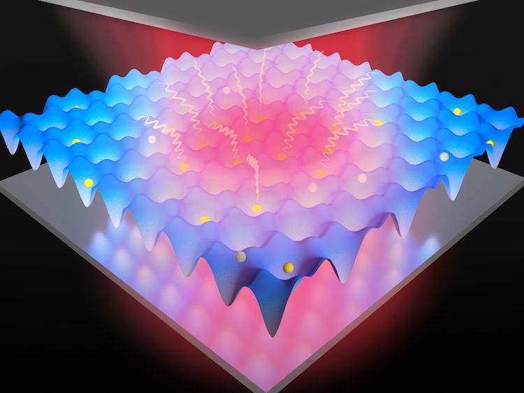
Interactions between matter and light in microcavities made of mirrors are fundamentally important for many modern technologies, including lasers. Researchers at the University of Michigan, Ann Arbor, US, have now gained tighter control of these interactions by exploiting a nonlinear effect that occurs in a new kind of hybrid semiconductor made from bilayers of two-dimensional materials. These semiconducting sheets form an egg-carton-like array in which the “pockets” are quantum dots that can be controlled using light, and they could be used to make ultralow-energy switches.

Led by Hui Deng, the researchers made their hybrid semiconductor from flakes of tungsten disulphide (WS2) and molybdenum diselenide (MoSe2) just a few atoms thick. In their bulk form, these transition-metal dichalcogenides (TMDCs) act as indirect band-gap semiconductors. When scaled down to a monolayer thickness, however, they behave as direct band-gap semiconductors, capable of efficiently absorbing and emitting light.

When laid on top of one another, the electronic structures of TMDCs can form a larger electron lattice (known as a moiré lattice) thanks to the slight mismatch of the materials’ lattice constants. The period of this lattice can be tuned by twisting the monolayers with respect to each other at different angles. In the WS2 and MoSe2 bilayer studied in this work, this angle is about 56.5° and the moiré lattice produced contains “pockets” measuring around 10 atoms across. These pockets, explains study lead author Long Zhang, are the quantum dots – tiny pieces of semiconducting materials that can isolate individual quantum particles such as electrons.

A team of researchers from QuTech in the Netherlands reports realization of the first multi-node quantum network, connecting three quantum processors. In addition, they achieved a proof-of-principle demonstration of key quantum network protocols. Their findings mark an important milestone toward the future quantum internet and have now been published in Science.

The power of the is that it allows any two computers on Earth to connect. Today, researchers in many labs around the world are working toward first versions of a quantum internet—a network that can connect any two , such as quantum computers or sensors, over large distances. Whereas today’s internet distributes information in bits that can be either 0 or 1, a future quantum internet will make use of quantum bits that can be 0 and 1 at the same time.

“A quantum internet will open up a range of novel applications, from unhackable communication and cloud computing with complete user privacy to high-precision time-keeping,” says Matteo Pompili, Ph.D. student and a member of the research team. “And like with the internet 40 years ago, there are probably many applications we cannot foresee right now.”

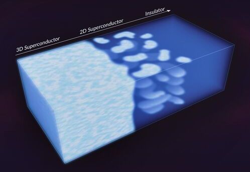
Creating a two-dimensional material, just a few atoms thick, is often an arduous process requiring sophisticated equipment. So scientists were surprised to see 2D puddles emerge inside a three-dimensional superconductor—a material that allows electrons to travel with 100% efficiency and zero resistance—with no prompting.

Within those puddles, superconducting electrons acted as if they were confined inside an incredibly thin, sheet-like plane, a situation that requires them to somehow cross over to another dimension, where different rules of quantum physics apply.

“This is a tantalizing example of emergent behavior, which is often difficult or impossible to replicate by trying to engineer it from scratch,” said Hari Manoharan, a professor at Stanford University and investigator with the Stanford Institute for Materials and Energy Sciences (SIMES) at the Department of Energy’s SLAC National Accelerator Laboratory, who led the research.

Ultralight bosons are hypothetical particles whose mass is predicted to be less than a billionth the mass of an electron. They interact relatively little with their surroundings and have thus far eluded searches to confirm their existence. If they exist, ultralight bosons such as axions would likely be a form of dark matter, the mysterious, invisible stuff that makes up 85 percent of the matter in the universe.

Now, physicists at MIT’s LIGO Laboratory have searched for ultralight bosons using black holes—objects that are mind-bending orders of magnitude more massive than the particles themselves. According to the predictions of quantum theory, a black hole of a certain mass should pull in clouds of ultralight bosons, which in turn should collectively slow down a black hole’s spin. If the particles exist, then all black holes of a particular mass should have relatively low spins.

But the physicists have found that two previously detected black holes are spinning too fast to have been affected by any ultralight bosons. Because of their large spins, the black holes’ existence rules out the existence of ultralight bosons with masses between 1.3×10⁻¹³ electronvolts and 2.7×10⁻¹³ electronvolts—around a quintillionth the mass of an electron.

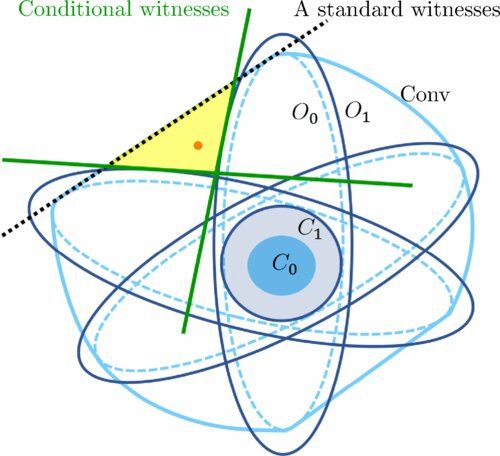
Physicists from Swansea University are part of an international research collaboration which has identified a new technique for testing the quality of quantum correlations.

Quantum computers run their algorithms on large quantum systems of many parts, called qubits, by creating quantum correlations across all of them. It is important to verify that the actual computation procedures lead to quantum correlations of desired quality.

However, carrying out these checks is resource-intensive as the number of tests required grows exponentially with the number of qubits involved.

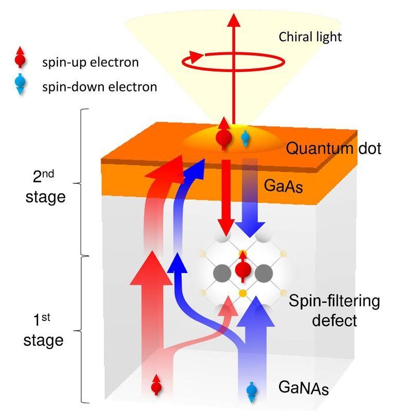
It may be possible in the future to use information technology where electron spin is used to store, process and transfer information in quantum computers. It has long been the goal of scientists to be able to use spin-based quantum information technology at room temperature. A team of researchers from Sweden, Finland and Japan have now constructed a semiconductor component in which information can be efficiently exchanged between electron spin and light at room temperature and above. The new method is described in an article published in Nature Photonics.

It is well known that electrons have a negative charge; they also have another property called spin. This may prove instrumental in the advance of . To put it simply, we can imagine the electron rotating around its own axis, similar to the way in which the Earth rotates around its own axis. Spintronics—a promising candidate for future information technology—uses this quantum property of electrons to store, process and transfer information. This brings important benefits, such as higher speed and lower energy consumption than traditional electronics.

Developments in spintronics in recent decades have been based on the use of metals, and these have been highly significant for the possibility of storing large amounts of data. There would, however, be several advantages in using spintronics based on semiconductors, in the same way that semiconductors form the backbone of today’s electronics and photonics.

Classical hydrodynamics laws can be very useful for describing the behavior of systems composed of many particles (i.e., many-body systems) after they reach a local state of equilibrium. These laws are expressed by so-called hydrodynamical equations, a set of mathematical equations that describe the movement of water or other fluids.

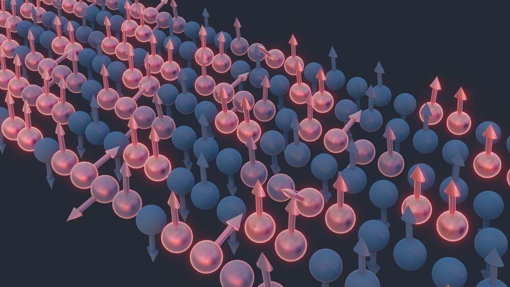
Researchers at Oak Ridge National Laboratory and University of California, Berkeley (UC Berkeley) have recently carried out a study exploring the hydrodynamics of a quantum Heisenberg spin-1/2 chain. Their paper, published in Nature Physics, shows that the spin dynamics of a 1D Heisenberg antiferromagnet (i.e., KCuF3) could be effectively described by a dynamical exponent aligned with the so-called Kardar-Parisi-Zhang universality class.

“Joel Moore and I have known each other for many years and we both have an interest in quantum magnets as a place where we can explore and test new ideas in physics; my interests are experimental and Joel’s are theoretical,” Alan Tennant, one of the researchers who carried out the study, told Phys.org. “For a long time, we have both been interested in temperature in quantum systems, an area where a number of really new insights have come along recently, but we had not worked together on any projects.”