Toggle light / dark theme

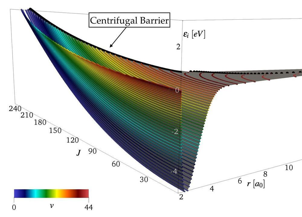
Hypersonic flight is conventionally referred to as the ability to fly at speeds significantly faster than the speed of sound and presents an extraordinary set of technical challenges. As an example, when a space capsule re-enters Earth’s atmosphere, it reaches hypersonic speeds—more than five times the speed of sound—and generates temperatures over 4,000 degrees Fahrenheit on its exterior surface. Designing a thermal protection system to keep astronauts and cargo safe requires an understanding at the molecular level of the complicated physics going on in the gas that flows around the vehicle.

Recent research at the University of Illinois Urbana-Champaign added new knowledge about the physical phenomena that occur as atoms vibrate, rotate, and collide in this extreme environment.

“Due to the relative velocity of the flow surrounding the vehicle, a shock is formed in front of the capsule. When the gas molecules cross the shock, some of their properties change almost instantaneously. Instead, others don’t have enough time to adjust to the abrupt changes, and they don’t reach their equilibrium values before arriving at the surface of the vehicle. The layer between the shock and heat shield is then found in nonequilibrium. There is a lot that we don’t understand yet about the reactions that happen in this type of flow,” said Simone Venturi. He is a graduate student studying with Marco Panesi in the Department of Aerospace Engineering at UIUC.

In the 1950s, few things seemed more futuristic and utopian than harnessing nuclear energy to power your home. Towering nuclear reactors popped up across the U.S. with the promise of harvesting energy from smashed atoms of Uranium to power everything from lights in an office to an oven cooking a pot roast. With clean and efficient nuclear power, anything seemed possible.

But as the years went on, doubt about the safety of these reactors began to poison the bright future they’d once promised. Stories of nuclear waste polluting waterways downstream of power plants began to stir alarm, and in the 1980s the Chernobyl nuclear power plant explosion sent radiation billowing across Europe and into the tissues of an estimated 4,000 Ukrainians who died from radiation poisoning. Even as recently as 2011, Japan’s Fukushima nuclear power plant faced catastrophe when a tsunami knocked out its power supply and led all three of its nuclear reactors to melt down.

All in all, it’s been a tough few decades for nuclear energy’s public image. But nuclear scientists say that now, more than ever, is the time to reinvest in nuclear innovation. Governments agree: In the U.K. Rolls-Royce plans to roll out 16 mini-nuclear plants over the next five years and China, an emerging nuclear super power, has pledged to ramp up its nuclear use to meet emissions goals.

You can’t see it. You can’t feel it. But the substance scientists refer to as dark matter could account for five times as much “stuff” in the universe as the regular matter that forms everything from trees, trains and the air you breathe, to stars, planets and interstellar dust clouds.

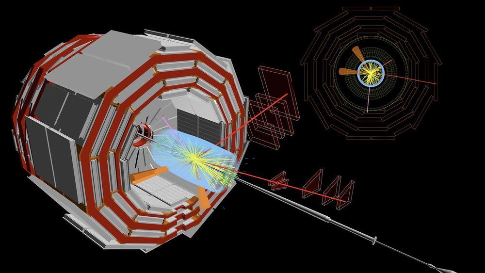
Though scientists see the signature of indirectly in the way large objects orbit one another—particularly how stars swirl around the centers of spiral galaxies—no one knows yet what comprises this substance. One of the candidates is a Z’ boson, a fundamental particle that has been theorized to exist but never detected.

A new proposed experiment could help scientists determine whether Z’ bosons are real, in that way identifying a possible candidate for dark matter. To accomplish this task, researchers from the National Institute of Standards and Technology (NIST), the University of Groningen in the Netherlands, the Canadian particle accelerator center TRIUMF and other collaborators are working to make the most to date of a nuclear property that is extremely difficult to measure, called nuclear spin-dependent parity violation (NSD-PV).

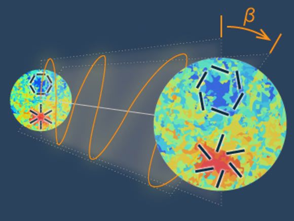
Using the polarization data from ESA’s Planck satellite, a mission that have studied the Cosmic Microwave Background (CMB), the oldest light in the Universe, a duo of astrophysicists has uncovered intriguing signs of new physics beyond the Standard Model of elementary particles and fields.

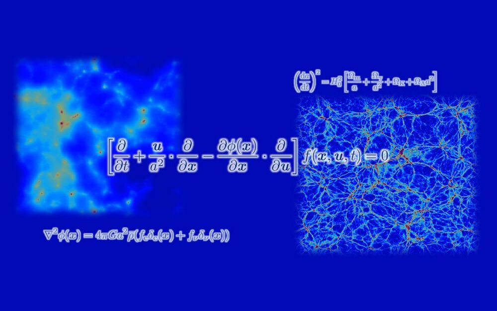
Computer simulations have struggled to capture the impact of elusive particles called neutrinos on the formation and growth of the large-scale structure of the universe. But now, a research team from Japan has developed a method that overcomes this hurdle.

In a study published this month in the Astrophysical Journal, researchers led by the University of Tsukuba present simulations that accurately depict the role of in the evolution of the universe.

Why are these simulations important? One key reason is that they can set constraints on a currently unknown quantity: the neutrino mass. If this quantity is set to a particular value in the simulations and the differ from observations, that value can be ruled out. However, the constraints can be trusted only if the simulations are accurate, which was not guaranteed in previous work. The team behind this latest research aimed to address this limitation.

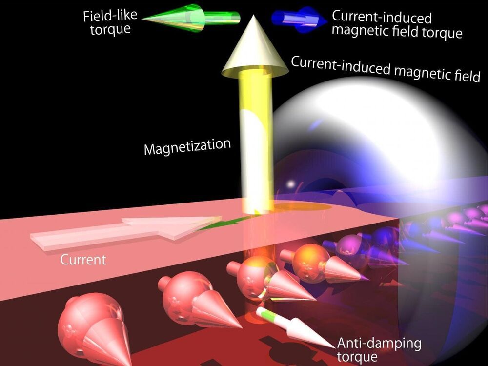
Researchers are a step closer to realizing a new kind of memory that works according to the principles of spintronics which is analogous to, but different from, electronics. Their unique gallium arsenide-based ferromagnetic semiconductor can act as memory by quickly switching its magnetic state in the presence of an induced current at low power. Previously, such current-induced magnetization switching was unstable and drew a lot of power, but this new material both suppresses the instability and lowers the power consumption too.

The field of quantum computing often gets covered in the technical press; however, another emerging field along similar lines tends to get overlooked, and that is spintronics. In a nutshell, spintronic devices could replace some and offer greater performance at far low power levels. Electronic devices use the motion of electrons for power and communication. Whereas use a transferable property of stationary electrons, their angular momentum, or spin. It’s a bit like having a line of people pass on a message from one to the other rather than have the person at one end run to the other. Spintronics reduces the effort needed to perform computational or memory functions.

Spintronic-based memory devices are likely to become common as they have a useful feature in that they are nonvolatile, meaning that once they are in a certain state, they maintain that state even without power. Conventional computer memory, such as DRAM and SRAM made of ordinary semiconductors, loses its state when it’s powered off. At the core of experimental spintronic devices are that can be magnetized in opposite directions to represent the familiar binary states of 1 or 0, and this switching of states can occur very, very quickly. However, there has been a long and arduous search for the best materials for this job, as magnetizing spintronic materials are no simple matter.

Researchers identify Brown-Zak fermions in superlattices made from the carbon sheet.


Researchers at the University of Manchester in the UK have identified a new family of quasiparticles in superlattices made from graphene sandwiched between two slabs of boron nitride. The work is important for fundamental studies of condensed-matter physics and could also lead to the development of improved transistors capable of operating at higher frequencies.

In recent years, physicists and materials scientists have been studying ways to use the weak (van der Waals) coupling between atomically thin layers of different crystals to create new materials in which electronic properties can be manipulated without chemical doping. The most famous example is graphene (a sheet of carbon just one atom thick) encapsulated between another 2D material, hexagonal boron nitride (hBN), which has a similar lattice constant. Since both materials also have similar hexagonal structures, regular moiré patterns (or “superlattices”) form when the two lattices are overlaid.

If the stacked layers of graphene-hBN are then twisted, and the angle between the two materials’ lattices decreases, the size of the superlattice increases. This causes electronic band gaps to develop through the formation of additional Bloch bands in the superlattice’s Brillouin zone (a mathematical construct that describes the fundamental ideas of electronic energy bands). In these Bloch bands, electrons move in a periodic electric potential that matches the lattice and do not interact with one another.

Faster, smaller, smarter and more energy-efficient chips for everything from consumer electronics to big data to brain-inspired computing could soon be on the way after engineers at The University of Texas at Austin created the smallest memory device yet. And in the process, they figured out the physics dynamic that unlocks dense memory storage capabilities for these tiny devices.

The research published recently in Nature Nanotechnology builds on a discovery from two years ago, when the researchers created what was then the thinnest storage device. In this new work, the researchers reduced the size even further, shrinking the cross section area down to just a single square nanometer.

Getting a handle on the physics that pack dense memory storage capability into these devices enabled the ability to make them much smaller. Defects, or holes in the material, provide the key to unlocking the high-density memory storage capability.

Scientists at Osaka University develop a label-free method for identifying respiratory viruses based on changes in electrical current when they pass through silicon nanopores, which may lead to new rapid COVID-19 tests.

The ongoing global pandemic has created an urgent need for rapid tests that can diagnose the presence of the SARS-CoV-2 virus, the pathogen that causes COVID-19, and distinguish it from other respiratory viruses. Now, researchers from Japan have demonstrated a new system for single-virion identification of common respiratory pathogens using a machine learning algorithm trained on changes in current across silicon nanopores. This work may lead to fast and accurate screening tests for diseases like COVID-19 and influenza.

In a study published this month in ACS Sensors scientists at Osaka University have introduced a new system using silicon nanopores sensitive enough to detect even a single virus particle when coupled with a machine learning algorithm.