Toggle light / dark theme

Taking inspiration from nature’s nanotech that creates the stunning color of butterfly wings, a University of Central Florida researcher is creating technology to make extremely low-power, ultra-high-definition displays and screens that are easier on the eyes.

The new technology creates digital displays that are lit by surrounding and are more natural looking than current display technologies that rely on energy-intensive bright lights hidden behind screens. The findings were published Wednesday in the journal Proceedings of the National Academy of Sciences.

“This display is more of a natural look than your current computer or smartphone screens,” said Debashis Chanda, an associate professor in UCF’s NanoScience Technology Center and principal investigator of the research. “It is like seeing a portrait on the wall at your house. It doesn’t have that glare or extra light. It is more like looking at the .”

Unprecedented View

The researchers believe this new nanoscale imaging technique could lead to the development of new materials and drugs, as well as the creation of better quantum computing systems.

“We can now see something that we couldn’t see before,” researcher Christopher Lutz told The New York Times. “So our imagination can go to a whole bunch of new ideas that we can test out with this technology.”

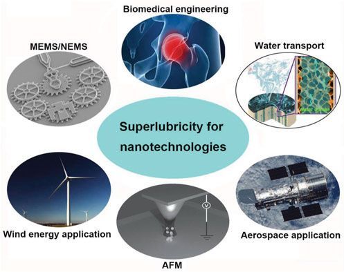
Achieving near-zero friction in commercial and industrial applications will be game-changing from tiny microelectromechanical systems that will never wear out, to oil-free bearings in industrial equipment, to much more efficient engines and giant wind turbines scavenging energy even in low wind conditions. Superlubricity offers promising solutions to overcome lubrication challenges in various areas of nanotechnology including micro/nano-electromechanical systems (MEMS/NEMS), water transport control, biomedical engineering, atomic force microscopy (AFM), aerospace and wind energy applications, as well as other electronic devices. It is one of the most promising properties of functional nanomaterials for energy saving applications.

Graphene, a two-dimensional honeycomb structure made of carbon atoms with a thickness of only one atom, has numerous outstanding properties. These include enormous mechanical resistance and extraordinary electronic and optical properties. Last year a team led by the Empa researcher Roman Fasel was able to show that it can even be magnetic: they succeeded in synthesizing a molecule in the shape of a bowtie, which has special magnetic properties.

Now, researchers report another breakthrough. Theoretical work from 2007 predicted that graphene could exhibit if it were cut into tiny triangles. Over the last three years, several teams, including the Empa team, have succeeded in producing the so-called triangulenes, consisting of only a few dozen , by chemical synthesis under ultra-high vacuum.

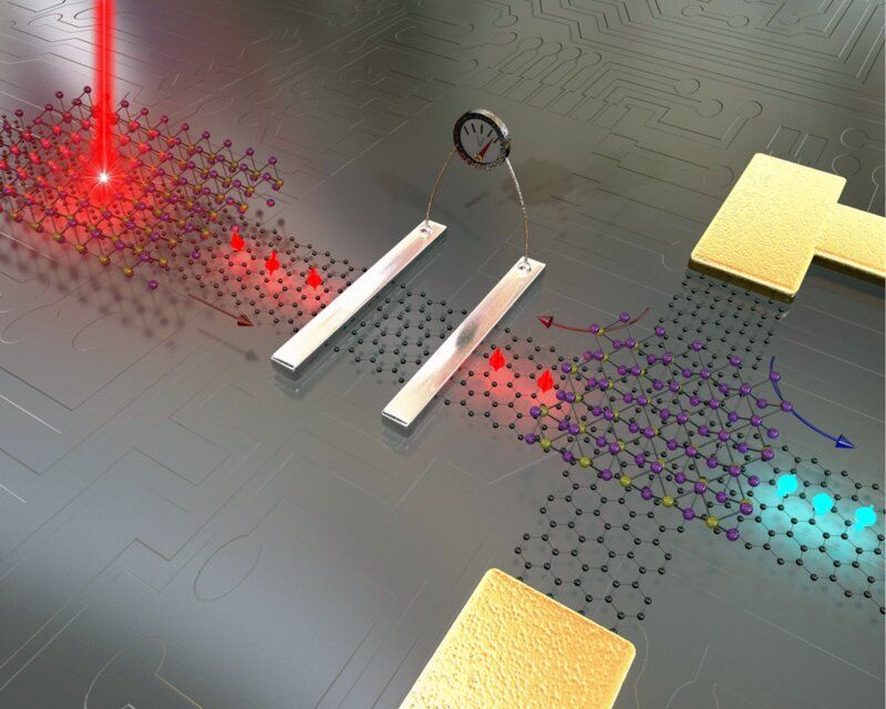
A team of researchers based in Manchester, the Netherlands, Singapore, Spain, Switzerland and the U.S. has published a new review on a field of computer device development known as spintronics, which could see graphene used as building block for next-generation electronics.

Recent theoretical and experimental advances and phenomena in studies of electronic spin transport in and related two-dimensional (2-D) materials have emerged as a fascinating area of research and development.

Spintronics is the combination of electronics and magnetism, at the nanoscale and could lead to next generation high-speed electronics. Spintronic devices are a viable alternative for nanoelectronics beyond Moore’s law, offering higher energy efficiency and lower dissipation as compared to conventional electronics, which relies on charge currents. In principle we could have phones and tablets operating with spin-based transistors and memories.

One of the biggest challenges for renewable energy research is energy storage. The goal is to find a material with high energy storage capacity and energy storage material with high storage capacity that can also quickly and efficiently discharge a large amount of energy. In an attempt to overcome this hurdle, researchers at the Queensland University of Technology (QUT) have proposed a brand-new carbon nanostructure designed to store energy in mechanical form.

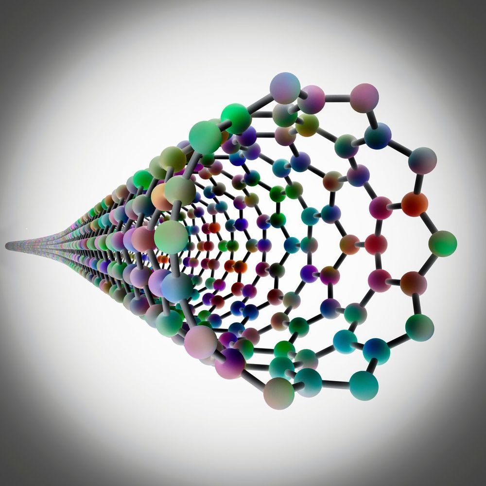
Most portable energy storage devices currently rely on storing energy in chemical form such as batteries, however this proposed new structure, made from a bundle of diamond nanothread (DNT) does not suffer from the same limiting properties as batteries, such as temperature sensitivity, or the potential to leak or explode. I have previously written about carbon nanotubes, and their applications in everything from Batman-like artificial muscle, to an analogy of the fictional element Vibranium, but a lot of research around carbon nanotubes is already focused on energy harvesting and energy storage applications.

What makes this energy storage method different is the method by which energy is stored, and also the related increased robustness of the resultant material. Dr Haifei Zhan and his team at the QUT Centre for material science used computer modelling to propose the structure of these ultra-thin one-dimensional carbon threads. The theory is that these threads should be able to store energy when they are twisted or stretched, similar to the way we store energy in wind-up toys. By turning the key, we force the spring inside into a tight coil. Once the key is released, the coil wishes to release the extra tension held within it and begins to unfurl. In doing so it transfers that mechanical energy into the movement of the toy’s wheels.

Customizable magnetic iron nanowires pinpoint and track the movements of target cells.

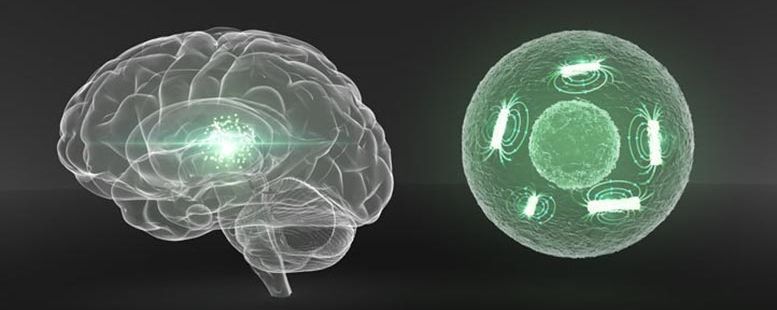
Living cells inside the body could be placed under surveillance—their location and migration noninvasively tracked in real time over many days—using a new method developed by researchers at KAUST.

The technique uses magnetic core-shell iron nanowires as nontoxic contrast agents, which can be implanted into live cells, lighting up those cells’ location inside a living organism when scanned by magnetic resonance imaging (MRI). The technique could have applications ranging from studying and treating cancer to tracking live-cell medical treatments, such as stem cell therapies.

Circa 2016


Researchers build “teeny, tiny structures” that can change infrared to visible light.

Remember that famous Bin Laden raid? It would have been impossible without night vision — specifically, a pair of $65,000 L-3 Ground Panoramic Night Vision Goggles. But even those top-of-the-line NVGs — former Navy SEAL Matt Bissonette compared other night-vision systems to “looking through toilet paper tubes” — are heavy, clunky, and odd-looking. Now researchers from Australia have developed a material that can make infrared light visible, raising the possibility of night-vision goggles as thin as glass and free of external power.

Conventional night vision goggles look a bit like binoculars and require electricity. Here’s how they work: An “objective lens” in front collects low-level and near-infrared light, whose photons are converted by a photocathode into electrons. The goggles use thousands of volts of electricity to send the electrons down a vacuum-sealed tube into a plate with millions of tiny holes. Pushing the electrons through the holes releases other electrons in a chain reaction called cascaded secondary emission. The effect: where there was one electron, there are now hundreds, all in the same pattern as the original photons. When the electrons hit the final layer, which is covered in phosphorescent material, what was dark becomes light.

The Norwegian Academy of Science and Letters today announced the 2020 Kavli Prize Laureates in the fields of astrophysics, nanoscience, and neuroscience. This year’s Kavli Prize honors scientists whose research has transformed our understanding of the very big, the very small and the very complex. The laureates in each field will share USD 1 million.

This year’s Kavli Prize Laureates are:

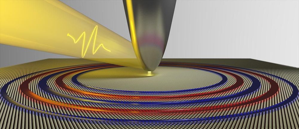
Study co-led by Berkeley Lab reveals how wavelike plasmons could power up a new class of sensing and photochemical technologies at the nanoscale.

Wavelike, collective oscillations of electrons known as “plasmons” are very important for determining the optical and electronic properties of metals.

In atomically thin 2D materials, plasmons have an energy that is more useful for applications, including sensors and communication devices, than plasmons found in bulk metals. But determining how long plasmons live and whether their energy and other properties can be controlled at the nanoscale (billionths of a meter) has eluded many.