Toggle light / dark theme

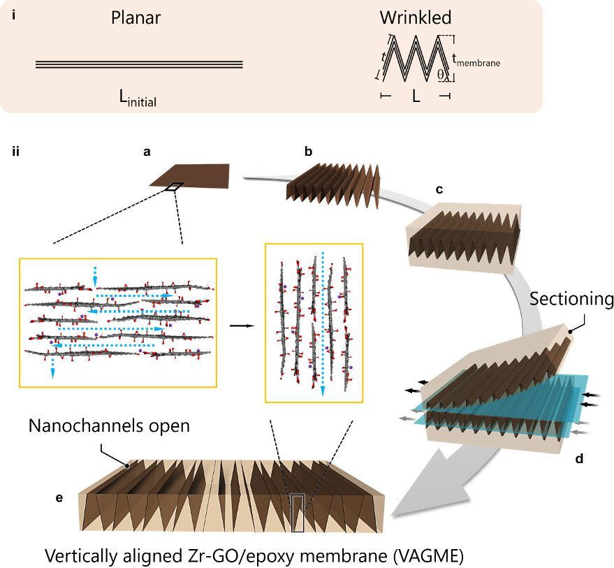
When sheets of two-dimensional nanomaterials like graphene are stacked on top of each other, tiny gaps form between the sheets that have a wide variety of potential uses. In research published in the journal Nature Communications, a team of Brown University researchers has found a way to orient those gaps, called nanochannels, in a way that makes them more useful for filtering water and other liquids of nanoscale contaminants.

“In the last decade, a whole field has sprung up to study these spaces that form between 2-D nanomaterials,” said Robert Hurt, a professor in Brown’s School of Engineering and coauthor of the research. “You can grow things in there, you can store things in there, and there’s this emerging field of nanofluidics where you’re using those channels to filter out some molecules while letting others go through.”

There’s a problem, however, with using these nanochannels for filtration, and it has to do with the way those channels are oriented. Like a notebook made from stacked sheets of paper, graphene stacks are thin in the vertical direction compared to their horizontal length and width. That means that the channels between the sheets are likewise oriented horizontally. That’s not ideal for filtration, because liquid has to travel a relatively long way to get from one end of a to the other. It would be better if the channels were perpendicular to the orientation of the sheets. In that case, liquid would only need to traverse the relatively thin vertical height of the stack rather than the much longer length and width.
The SonoMask displayed an ability to neutralize the novel coronavirus at an effectiveness of 99.34% within trials performed by the ATCCR Testing laboratory in China, Ramat Gan-based Israeli fabric maker and developer Sonovia announced on Saturday. Sonovia’s reusable anti-viral masks are coated in zinc oxide nanoparticles that destroy bacteria, fungi and viruses, which it says can help stop the spread of the coronavirus. Results from the most recent round of testing showed that the mask has the ability to neutralize fallen traces of SARS-COV-2 within 30 minutes after making contact with the fabric. The SonoMask was also proven to maintain its protective properties throughout 55 wash cycles.” Following this outstanding result – the product of several months of dedicated anti-viral sonochemistry formulation – we can now assure the public that our SonoMask is working continuously, permanently and rapidly to neutralize the spread of COVID-19,” said Sonovia CEO Joshua Hershcovici. “We are proud of our latest accomplishment that will help people feel safe and protect their loved ones, all the while remaining the most ecologically sound option upon the PPE market.” Sonovia also participated in trials with Adler Plastic in Italy earlier this year, working toward creating a solution for carpets and other types of fabrics. The company boasted a 99.999% efficiency rate against bacteria during the pilot testing round. Furthermore, the Israeli fabric maker has attracted the cooperation of top brands such as Gucci, Chanel and Adidas, working on the Fashion for Good Plug and Play accelerator project – and earning a $250000 investment for their innovation.” We see our breakthrough technology transforming our everyday life, implemented in all textiles surrounding us: from the clothes we wear, to the textiles in our home, the textiles in our public spaces, in public transportation and of course as a protective measure in the workplaces & medical institutes – in a manner that ensures safer surroundings during these unusual times,” said Sonovia’s Chief Technology Officer Liat Goldhammer.

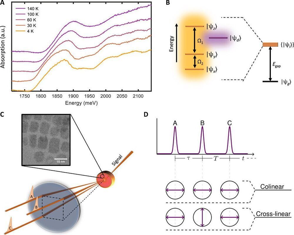
Advanced optoelectronics require materials with newly engineered characteristics. Examples include a class of materials named metal-halide perovskites that have tremendous significance to form perovskite solar cells with photovoltaic efficiencies. Recent advances have also applied perovskite nanocrystals in light-emitting devices. The unusually efficient light emission of cesium lead-halide perovskite may be due to a unique excitonic fine structure made of three bright triplet states that minimally interact with a proximal dark singlet state. Excitons are electronic excitations responsible for the emissive properties of nanostructured semiconductors, where the lowest-energy excitonic state is expected to be long lived and hence poorly emitting (or ‘dark’).

In a new report now published in Science Advances, Albert Liu and a team of scientists in physics and chemistry at the University of Michigan, U.S., and Campinas State University, Brazil, used multidimensional coherent spectroscopy at cryogenic (ultra-cold) temperatures to study the fine structure without isolating the cube-shaped single . The work revealed coherences (wave properties relative to space and time) involving the triplet states of a cesium lead-iodide (CsPbI3) nanocrystal ensemble. Based on the measurements of triplet and inter-triplet coherences, the team obtained a unique exciton fine structure level ordering composed of a dark state, energetically positioned within the bright triplet manifold.

Exotic and vibrant colors naturally occur in nature because of pigmentations. But nature is also capable of displaying a whole spectrum of eye-catching colors through building nano-scale surface structures. Creatures with intricate physical aesthetics, like a peacock’s feathers or the rich patterns on a butterfly’s wings, achieve this kind of high color resolution due to the small-scale arrays of distinctly shaped objects on their surfaces. This naturally occurring color structure was exploited by a team of researchers from the Technical University of Denmark (DTU). They developed a laser printing technique that doesn’t require ink.

Laser printing without ink

A laser printing technique developed by Anders Kristensen and his DTU team is able to produce high-resolution images without fading away and without using any ink. The team constructed a material called metasurface, which consists of 60 nanometers high columns of plastic. The material’s surface is painted with a coating of germanium, of only 35 nanometers in thickness, then semiconductors are placed on top of the pillars or columns.

A team of biophysicists from the University of Massachusetts Amherst and Penn State College of Medicine set out to tackle the long-standing question about the nature of force generation by myosin, the molecular motor responsible for muscle contraction and many other cellular processes. The key question they addressed—one of the most controversial topics in the field—was: how does myosin convert chemical energy, in the form of ATP, into mechanical work?

The answer revealed new details into how myosin, the engine of muscle and related motor proteins, transduces energy.

In the end, their unprecedented research, meticulously repeated with different controls and double-checked, supported their hypothesis that the mechanical events of a precede—rather than follow—the biochemical events, directly challenging the long-held view that biochemical events gate the force-generating event. The work, published in the Journal of Biological Chemistry, was selected as an Editor’s Pick for “providing an exceptional contribution to the field.”

Researchers develop the first nanomaterial that demonstrates “photon avalanching;” finding could lead to new applications in sensing, imaging, and light detection.

Researchers at Columbia Engineering report today that they have developed the first nanomaterial that demonstrates “photon avalanching,” a process that is unrivaled in its combination of extreme nonlinear optical behavior and efficiency. The realization of photon avalanching in nanoparticle form opens up a host of sought-after applications, from real-time super-resolution optical microscopy, precise temperature and environmental sensing, and infrared light detection, to optical analog-to-digital conversion and quantum sensing.

“Nobody has seen avalanching behavior like this in nanomaterials before,” said James Schuck, associate professor of mechanical engineering, who led the study published today (January 132021) by Nature. “We studied these new nanoparticles at the single-nanoparticle level, allowing us to prove that avalanching behavior can occur in nanomaterials. This exquisite sensitivity could be incredibly transformative. For instance, imagine if we could sense changes in our chemical surroundings, like variations in or the actual presence of molecular species. We might even be able to detect coronavirus and other diseases.”

Researchers at Columbia Engineering report today that they have developed the first nanomaterial that demonstrates “photon avalanching,” a process that is unrivaled in its combination of extreme nonlinear optical behavior and efficiency. The realization of photon avalanching in nanoparticle form opens up a host of sought-after applications, from real-time super-resolution optical microscopy, precise temperature and environmental sensing, and infrared light detection, to optical analog-to-digital conversion and quantum sensing.

“Nobody has seen avalanching behavior like this in nanomaterials before,” said James Schuck, associate professor of mechanical engineering, who led the study published today by Nature. “We studied these new nanoparticles at the single-nanoparticle level, allowing us to prove that avalanching behavior can occur in nanomaterials. This exquisite sensitivity could be incredibly transformative. For instance, imagine if we could sense changes in our chemical surroundings, like variations in or the actual presence of molecular species. We might even be able to detect coronavirus and other diseases.”

Avalanching processes—where a cascade of events is triggered by series of small perturbations—are found in a wide range of phenomena beyond snow slides, including the popping of champagne bubbles, nuclear explosions, lasing, neuronal networking, and even financial crises. Avalanching is an extreme example of a nonlinear process, in which a change in input or excitation leads to a disproportionate—often disproportionately large—change in output signal. Large volumes of material are usually required for the efficient generation of nonlinear optical signals, and this had also been the case for avalanching, until now.

While many research teams worldwide are trying to develop highly performing quantum computers, some are working on tools to control the flow of heat inside of them. Just like conventional computers, in fact, quantum computers can heat up significantly as they are operating, which can ultimately damage both the devices and their surroundings.

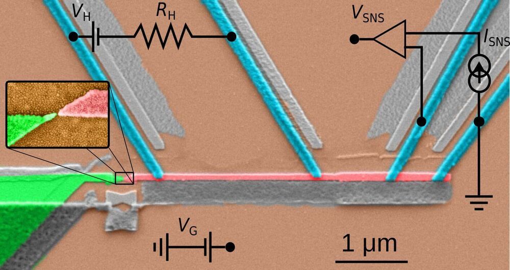
A team of researchers at University Grenoble Alpes in France and Centre of Excellence—Quantum Technology in Finland has recently developed a single-quantum-dot heat valve, a that can help to control the flow of heat in single-quantum-dot junctions. This heat valve, presented in a paper published in Physical Review Letters, could help to prevent quantum computers from overheating.

“With the miniaturization of electronic components handling of excess heat at nanoscales has become an increasingly important issue to be addressed,” Nicola Lo Gullo, one of the researchers who carried out the study, told Phys.org. “This is especially true when one wants to preserve the quantum nature of a device; the increase in temperature does typically result in the degradation of the quantum properties. The recent realization of a photonic heat-valve by another research group ultimately inspired us to create a heat valve based on a solid-state quantum dot.”

A team led by University of Minnesota Twin Cities researchers has discovered a groundbreaking one-step process for creating materials with unique properties, called metamaterials. Their results show the realistic possibility of designing similar self-assembled structures with the potential of creating “built-to-order” nanostructures for wide application in electronics and optical devices.

The research was published and featured on the cover of Nano Letters, a peer-reviewed scientific journal published by the American Chemical Society.

In general, metamaterials are made in the lab so as to provide specific physical, chemical, electrical, and optical properties otherwise impossible to find in naturally occurring materials. These materials can have which make them ideal for a variety of applications from optical filters and medical devices to aircraft soundproofing and infrastructure monitoring. Usually these nano-scale materials are painstakingly produced in a specialized clean room environment over days and weeks in a multi-step fabrication process.

In a technique known as DNA origami, researchers fold long strands of DNA over and over again to construct a variety of tiny 3D structures, including miniature biosensors and drug-delivery containers. Pioneered at the California Institute of Technology in 2006, DNA origami has attracted hundreds of new researchers over the past decade, eager to build receptacles and sensors that could detect and treat disease in the human body, assess the environmental impact of pollutants, and assist in a host of other biological applications.

Although the principles of DNA are straightforward, the technique’s tools and methods for designing new structures are not always easy to grasp and have not been well documented. In addition, scientists new to the method have had no single reference they could turn to for the most efficient way of building DNA structures and how to avoid pitfalls that could waste months or even years of research.

That’s why Jacob Majikes and Alex Liddle, researchers at the National Institute of Standards and Technology (NIST) who have studied DNA origami for years, have compiled the first detailed tutorial on the technique. Their comprehensive report provides a step-by-step guide to designing DNA origami nanostructures, using state-of-the-art tools. Majikes and Liddle described their work in the Jan .8 issue of the Journal of Research of the National Institute of Standards and Technology.