Toggle light / dark theme

In semiconductor device applications, there is an increasing demand for semiconductors with very high carrier concentrations. The semiconductor material parameters, namely carrier density and mobility, primarily determine device performance. Hence, it is important to accurately characterize the carrier density and mobility of a semiconductor for the development of its device applications.
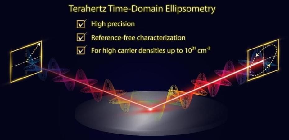
The use of THz waves, or with wavelengths of around 300 µm and frequency of about 1 THz, in the nondestructive testing of semiconductors has been continuously expanding. Free carriers in a material absorb THz radiation, which makes it possible to estimate the electrical properties of semiconductors using THz waves.

Researchers at Osaka University, in collaboration with Nippo Precision Co., Ltd., developed a THz time-domain ellipsometry system (Tera Evaluator) that extends the range of carrier concentrations measurable by THz waves up to ~1020 cm-3 and potentially higher by improving the precision of said optical technique. In THz time-domain ellipsometry, linearly polarized THz pulses are incident on a sample and the electric field strength of the reflected THz waves as a function of time is measured. Specifically, the reflected waves polarized in the direction parallel ℗ and perpendicular (s) to the plane of incidence are of interest. The ratio of the p-and s-polarization components yields information on the electric permittivity of the sample, allowing for the evaluation of the carrier density and mobility. As such, unlike THz time-domain spectroscopy, THz time-domain ellipsometry does not require reference measurements through an aperture or standard mirror.

https://youtube.com/watch?v=FiU5U_6ca0s

Of all the different dark matter detectors in the world, only one has consistently come up with a positive signal. The results of DAMA experiment in Italy are hotly debated — and now two experiments seeking to verify it using the same materials have returned conflicting results.

ANAIS, a dark matter detector run by the University of Zaragoza at the Canfranc Underground Laboratory in Spain, has delivered results that seem to contradict DAMA’s.

But COSINE-100, run by a collaboration between the Korea Invisible Mass Search and Yale University at the Yangyang Underground Laboratory in South Korea, has now produced new output. These results are similar to what ANAIS’ threw up — but also a little closer to the results DAMA has produced over the last 20 years.

Like ripples in a pond, electrons travel like waves through materials, and when they collide and interact, they can give rise to new and interesting patterns.

Scientists at the U.S. Department of Energy’s (DOE) Argonne National Laboratory have seen a new kind of wave pattern emerge in a thin film of metal oxide known as titania when its shape is confined. Confinement, the act of restricting materials within a boundary, can alter the properties of a material and the movement of molecules through it.

In the case of titania, it caused electrons to interfere with each other in a unique pattern, which increased the oxide’s conductivity, or the degree to which it conducts electricity. This all happened at the mesoscale, a scale where scientists can see both quantum effects and the movement of electrons and molecules.

In a press statement from the UK government, the work is described as a “world first.” The material is being used as part of a trial, meaning that the UK government will keep a close eye on the newly-laid surface over the coming years to discern whether graphene can be used more widely to increase the durability and lifespan of roads.


The concept has been meticulously tested in labs, now it’s time for a real-world application.

We all know that light and sound are wave phenomena, but of very different kinds. Light is electromechanical in nature, while sound is mechanical. Light can travel through a vacuum, while sound needs some sort of medium to transmit it. So it would seem that it might be difficult to use sound to modify light, but with the right equipment, it’s actually pretty easy.

Easy, perhaps, if you’re used to slinging lasers around and terms like “acousto-optic tunable filter” fall trippingly from your tongue, as is the case for [Les Wright]. An AOTF is a device that takes a radio frequency input and applies it to a piezoelectric transducer that’s bonded to a crystal of tellurium oxide. The RF signal excites the transducer, which vibrates the TeO2 crystal and sets up a standing wave within it. The alternating bands of compressed and expanded material within the crystal act like a diffraction grating. Change the excitation frequency, and the filter’s frequency changes too.

To explore the way sound can bend light, [Les] picked up a commercial AOTF from the surplus market. Sadly, it didn’t come with the RF driver, but no matter — a few quick eBay purchases put the needed RF generator and power amplifier on his bench. The modules went into an enclosure to make the driver more of an instrument and less of a one-off, with a nice multi-turn pot and vernier knob for precise filter adjustment. It’s really kind of cool to watch the output beam change colors at the twist of a knob, and cooler still to realize how it all works.

Most integrated circuits (ICs) and electronic components developed to date are based on silicon metal-oxide-semiconductor (CMOS) technology. As silicon (Si) is known to have a narrow bandgap, however, in recent years engineers have been trying to develop ICs using other materials with a wider bandgap, such as gallium nitrite (GaN).

ICs made of GaN could have notable advantages over conventional ICs based on silicon, particularly for the development of power electronics, radiofrequency power amplifiers and devices designed to operate in harsh environments. However, so far developing GaN CMOS has proved to be highly challenging, due to the intrinsically low mobility of holes in the material and the lack of a suitable strategy for integrating n-channel and p-channel field-effect transistors (n-FETs and p-FETs) on a single substrate.

Researchers at the Hong Kong University of Science and Technology (HKUST) have recently realized a series of GaN-based complementary logic ICs. Their paper, published in Nature Electronics, could have important implications for the development of new types of electronics.

Mott Insulator Exhibits a Sharp Response to Electron Injection In a finding that will give theorists plenty to ponder, an all-RIKEN team has observed an unexpected response in an exotic material known as a Mott insulator when they injected electrons into it. This observation promises to give physicists new insights into such materials, which are closely related to high-temperature superconductors.