Toggle light / dark theme

DARPA Looks to Light up Integrated Photonics with Chip-Scale Laser Development

DARPA Looks to Light up Integrated Photonics with Chip-Scale Laser DevelopmentAgency announces performer teams selected for LUMOS program.

Like.

Comment.


First demonstrated sixty years ago, the laser has become an essential technology in today’s world. It has transformed diverse fields including communications, sensing, manufacturing, and medicine. More recently, innovations in integrated photonics have allowed the miniaturization of key optical components and the ability to arrange several elements on a single silicon chip. When combined with lasers, these photonic integrated circuits (PICs) have the potential to replace large and costly optical systems with chip-scale solutions. However, due to differences in the properties of the materials that compose them, lasers and PICs are difficult to combine onto the same platform, limiting the benefits of integration and preventing broad technology impact.

To address this challenge, DARPA developed the Lasers for Universal Microscale Optical Systems (LUMOS) program, which aims to bring high-performance lasers to advanced photonics platforms. As highlighted in the recent program kick-off meeting, LUMOS will address several commercial and defense applications by directing efforts across three distinct Technical Areas.

The first LUMOS Technical Area brings high-performance lasers and optical amplifiers into advanced domestic photonics manufacturing foundries. Two research teams were selected in this area: Tower Semiconductor and SUNY Polytechnic Institute. These performers will work to demonstrate flexible, efficient on-chip optical gain in their photonics processes to enable next-generation optical microsystems for communications, computing, and sensing. LUMOS technologies will be made available to future design teams through DARPA-sponsored multi-project wafer runs.

Scientists unveil latest femtosecond laser

Would you like to capture a chemical transformation inside a cell live? Or maybe revolutionize microchips’ production by printing paths in a layer that has a thickness of just 100 nanometers? These and many other goals can now be achieved with the latest femtosecond laser created by a team of scientists led by Dr. Yuriy Stepanenko.

These days, there is a multitude of laser light sources. They each have their characteristics and different applications, such as observing stars, treating illnesses, and surface micro-machining. “Our goal is to develop new ones,” says Yuriy Stepanenko, head of the team of Ultrafast Laser Techniques at the Institute of Physical Chemistry of the Polish Academy of Sciences. “We deal with sources that produce ultrashort pulses of light. Really very, very short—femtosecond pulses (that’s a part of a second with 15 zeros after the decimal point). This is the scale on which, for example, intracellular chemical reactions take place. To see them, we have to ” take a photo” in this very short time. And thanks to the new laser, we can do just that.

We can also use our source for the very precise removal of materials from various surfaces without destroying them, says the scientist. We could, for example, clean the Mona Lisa using this method without damaging the layers of paint. We would only remove dust and dirt, a layer about 10 nanometers thick, explains Dr. Stepanenko, one of the authors of a study recently published in the Journal of Lightwave Technology.

Quantum Entanglement of Electrons Using Heat

Quantum entanglement is key for next-generation computing and communications technology, Aalto researchers can now produce it using temperature differences.

A joint group of scientists from Finland, Russia, China, and the USA have demonstrated that temperature difference can be used to entangle pairs of electrons in superconducting structures. The experimental discovery, published in Nature Communications, promises powerful applications in quantum devices, bringing us one step closer towards applications of the second quantum revolution.

The team, led by Professor Pertti Hakonen from Aalto University, has shown that the thermoelectric effect provides a new method for producing entangled electrons in a new device. “Quantum entanglement is the cornerstone of the novel quantum technologies. This concept, however, has puzzled many physicists over the years, including Albert Einstein who worried a lot about the spooky interaction at a distance that it causes,” says Prof. Hakonen.

Sci-Fi UI Episode 1: The Expanse

In this episode of Sci-Fi UI, we’ll find out whether the computer interfaces in The Expanse can actually be built in the real world. In Sci-Fi UI, we deep-dive into the UI of tomorrow to see if we can learn anything about building better UI today.

Narrated by:
AJ Campbell.

Twitter:
http://twitter.com/texasgreentea.

Portfolio:
http://ajcampbell.info.

Attribution:

Oculus Quest Hand Tracking Review:

Engineers find antioxidants improve nanoscale visualization of polymers

Reactive molecules, such as free radicals, can be produced in the body after exposure to certain environments or substances and go on to cause cell damage. Antioxidants can minimize this damage by interacting with the radicals before they affect cells.

Led by Enrique Gomez, professor of chemical engineering and and engineering, Penn State researchers have applied this concept to prevent imaging damage to conducting polymers that comprise soft electronic devices, such as , organic transistors, bioelectronic devices and flexible electronics. The researchers published their findings in Nature Communications today (Jan. 8).

According to Gomez, visualizing the structures of conducting polymers is crucial to further develop these materials and enable commercialization of soft electronic devices—but the actual imaging can cause damage that limits what researchers can see and understand.

The World’s First Quantum Phase Battery Is Here

O,.o circa 2020.


Their quantum phase battery consists of an n-doped InAs nanowire forming the core of the battery (the pile) and Al superconducting leads as poles. It is charged by applying an external magnetic field, which then can be switched off.

Cristina Sanz-Fernández and Claudio Guarcello, also from CFM, adapted the theory to simulate the experimental findings.

The battery is being further developed and improved at CFM premises in a collaboration between the Nanophysics Lab and the Mesoscopic Physics Group. These advances could contribute to enormous advances that many say will come from the field of quantum computing.

Researchers question fundamental study on the Kondo effect

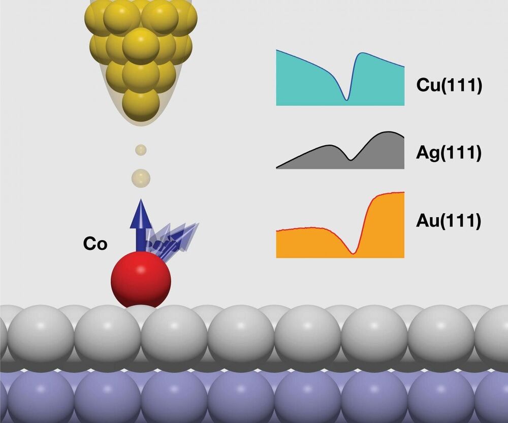
The Kondo effect influences the electrical resistance of metals at low temperatures and generates complex electronic and magnetic orders. Novel concepts for data storage and processing, such as using quantum dots, are based on this. In 1998, researchers from the United States published spectroscopic studies on the Kondo effect using scanning tunneling microscopy, which are considered ground-breaking and have triggered countless others of a similar kind. Many of these studies may have to be re-examined now that Jülich researchers have shown that the Kondo effect cannot be proven beyond doubt by this method. Instead, another phenomenon is creating precisely the spectroscopic ‘fingerprint’ that was previously attributed to the Kondo effect.

Normally the resistance of metals decreases as the temperature drops. The Kondo effect causes it to rise again below a threshold value typical to the material in question, the so-called Kondo temperature. This phenomenon occurs when magnetic foreign atoms, such as iron, contaminate non-magnetic host metals, such as copper. Simply put, when a current flows, the atomic nuclei are engulfed by electrons. The iron atoms have a quantum mechanical magnetic moment. This causes the electrons in the vicinity to align their spin antiparallel to the moment of the atom at low temperatures and to hang around the cobalt atom like a cloud on a mountaintop. This hinders the flow of the electrons—the electrical resistance then increases. In physics, this is known as entanglement, the strong coupling of the moment of the impurity with the spins of the surrounding electrons.

2020’s Biggest Breakthroughs in Math and Computer Science

For mathematicians and computer scientists, 2020 was full of discipline-spanning discoveries and celebrations of creativity. We’d like to take a moment to recognize some of these achievements.

1. A landmark proof simply titled MIP = RE” establishes that quantum computers calculating with entangled qubits can theoretically verify the answers to an enormous set of problems. Along the way, the five computer scientists who authored the proof also answered two other major questions: Tsirelson’s problem in physics, about models of particle entanglement, and a problem in pure mathematics called the Connes embedding conjecture.

2. In February, graduate student Lisa Piccirillo dusted off some long-known but little-utilized mathematical tools to answer a decades-old question about knots. A particular knot named after the legendary mathematician John Conway had long evaded mathematical classification in terms of a higher-dimensional property known as sliceness. But by developing a version of the knot that yielded to traditional knot analysis, Piccirillo finally determined that the Conway knot is not slice.

3. For decades, mathematicians have used computer programs known as proof assistants to help them write proofs — but the humans have always guided the process, choosing the proof’s overall strategy and approach. That may soon change. Many mathematicians are excited about a proof assistant called Lean, an efficient and addictive proof assistant that could one day help tackle major problems. First, though, mathematicians must digitize thousands of years of mathematical knowledge, much of it unwritten, into a form Lean can process. Researchers have already encoded some of the most complicated mathematical ideas, proving in theory that the software can handle the hard stuff. Now it’s just a question of filling in the rest.

Physicists observe competition between magnetic orders

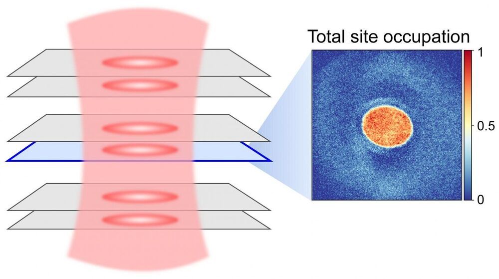
They are as thin as a hair, only a hundred thousand times thinner—so-called two-dimensional materials, consisting of a single layer of atoms, have been booming in research for years. They became known to a wider audience when two Russian-British scientists were awarded the Nobel Prize in Physics in 2010 for the discovery of graphene, a building block of graphite. The special feature of such materials is that they possess novel properties that can only be explained with the help of the laws of quantum mechanics and that may be relevant for enhanced technologies. Researchers at the University of Bonn (Germany) have now used ultracold atoms to gain new insights into previously unknown quantum phenomena. They found out that the magnetic orders between two coupled thin films of atoms compete with each other. The study has been published in the journal Nature.

Quantum systems realize very unique states of matter originating from the world of nanostructures. They facilitate a wide variety of new technological applications, e.g. contributing to secure data encryption, introducing ever smaller and faster technical devices and even enabling the development of a quantum computer. In the future, such a computer could solve problems which conventional computers cannot solve at all or only over a long period of time.

How unusual quantum phenomena arise is still far from being fully understood. To shed light on this, a team of physicists led by Prof. Michael Köhl at the Matter and Light for Quantum Computing Cluster of Excellence at the University of Bonn are using so-called quantum simulators, which mimic the interaction of several quantum particles—something that cannot be done with conventional methods. Even state-of-the-art computer models cannot calculate complex processes such as magnetism and electricity down to the last detail.