Toggle light / dark theme

This article is part of a series tracking the effects of the COVID-19 pandemic on major businesses and sectors. For other articles and earlier versions, go here.

A global shortage of semiconductors — chips that power massive data-centers, modern autos and countless digital devices — has roiled global manufacturing and is not expected to end soon. It isn’t a blanket problem, however, as different sectors within the chip industry will continue to be affected by the shortage in different ways.

As the industry entered 2020, high demand was expected in the mobile chip area because of the rollout of 5G devices. That path was turned on its head when COVID-19 became a global pandemic, driving millions, if not billions, of people into the safety of their homes to work, go to school, be entertained and to socialize.


Sorry, we’re having trouble playing this video.

Learn More.

World Economic Forum.

· —6-h ·

A call to protect the planet 📱

🔎 Learn more about the rise in e-waste.


It’s hard to imagine navigating modern life without a mobile phone in hand. Computers, tablets and smartphones have transformed how we communicate, work, learn, share news and entertain ourselves. They became even more essential when the COVID-19 pandemic moved classes, meetings and social connections online.

But few people realize that our reliance on electronics comes with steep environmental costs, from mining minerals to disposing of used devices. Consumers can’t resist faster products with more storage and better cameras, but constant upgrades have created a growing global waste challenge. In 2019 alone, people discarded 53 million metric tons of electronic waste.

In our work as sustainability researchers, we study how consumer behavior and technological innovations influence the products that people buy, how long they keep them and how these items are reused or recycled.

Encoding information into light, and transmitting it through optical fibers lies at the core of optical communications. With an incredibly low loss of 0.2 dB/km, optical fibers made from silica have laid the foundations of today’s global telecommunication networks and our information society.

Such ultralow optical loss is equally essential for integrated photonics, which enable the synthesis, processing and detection of optical signals using on-chip waveguides. Today, a number of innovative technologies are based on integrated photonics, including semiconductor lasers, modulators, and photodetectors, and are used extensively in data centers, communications, sensing and computing.

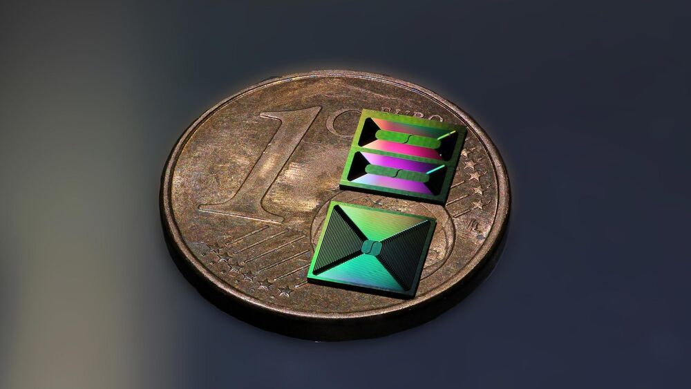
Integrated photonic chips are usually made from silicon that is abundant and has good optical properties. But silicon can’t do everything we need in integrated photonics, so new material platforms have emerged. One of these is silicon nitride (Si3N4), whose exceptionally low optical loss (orders of magnitude lower than that of silicon), has made it the material of choice for applications for which low loss is critical, such as narrow-linewidth lasers, photonic delay lines, and nonlinear photonics.

Spin waves could unlock the next generation of computer technology, a new component allows physicists to control them.

Researchers at Aalto University have developed a new device for spintronics. The results have been published in the journal Nature Communications, and mark a step towards the goal of using spintronics to make computer chips and devices for data processing and communication technology that are small and powerful.

Traditional electronics uses electrical charge to carry out computations that power most of our day-to-day technology. However, engineers are unable to make electronics do calculations faster, as moving charge creates heat, and we’re at the limits of how small and fast chips can get before overheating. Because electronics can’t be made smaller, there are concerns that computers won’t be able to get more powerful and cheaper at the same rate they have been for the past 7 decades. This is where spintronics comes in.

January 25, 2021


CAMBRIDGE, England, Jan. 25, 2021 — Riverlane, a quantum software company, today announces that it has raised $20m in Series A funding to build Deltaflow, its operating system for quantum computers. Over the past year, Riverlane has signed up 20% of the world’s quantum hardware manufacturers to use Deltaflow and will use the funding to expand internationally to the US, Europe and beyond.

The round was led by European technology venture capital fund Draper Esprit, and supported by existing investors, Cambridge Innovation Capital, Amadeus Capital Partners, and the University of Cambridge.

Quantum computers will change the world by solving problems that are fundamentally impossible to solve on classical computers. This step change in computing power will have an enormous impact on a variety of industries, for example the pharmaceuticals and materials industry. Over the next five years we will continue to see rapid progress in quantum hardware development and, as the quantum industry develops, it’s vital that software is built on a solid foundation.

Amazon Web Services (AWS) is partnering with the Hebrew University of Jerusalem for a new quantum computing initiative as part of the company’s efforts, launched in 2019, to explore this area of research. These include a cloud-based quantum computing service Amazon Braket to accelerate research and discovery, the Amazon Quantum Solutions Lab to help businesses explore quantum applications, and the AWS Center for Quantum Computing research and development organization.

AWS’ latest collaboration with Hebrew University will fund a team of researchers from the academic institution’s Quantum Information Science Center (QISC), founded in 2013, and the Racah Institute of Physics to advance the understanding of quantum gates – fundamental building blocks of quantum computers, the parties said in a statement on Monday. The collaboration is the first between AWS and any Israeli academic institution in the field.

The university’s Professor Alex Retzker, a researcher of quantum technologies, will lead the research group as part of his role as a Principal Research Scientist at AWS.

Yesterday Nvidia officially dipped a toe into quantum computing with the launch of cuQuantum SDK, a development platform for simulating quantum circuits on GPU-accelerated systems. As Nvidia CEO Jensen Huang emphasized in his keynote, Nvidia doesn’t plan to build quantum computers, but thinks GPU-accelerated platforms are the best systems for quantum circuit and algorithm development and testing.

As a proof point, Nvidia reported it collaborated with Caltech to develop “a state-of-the-art quantum circuit simulator with cuQuantum running on NVIDIA A100 Tensor Core GPUs. It generated a sample from a full-circuit simulation of the Google Sycamore circuit in 9.3 minutes on Selene, a task that 18 months ago experts thought would take days using millions of CPU cores.”

A team of researchers from QuTech in the Netherlands reports realization of the first multi-node quantum network, connecting three quantum processors. In addition, they achieved a proof-of-principle demonstration of key quantum network protocols. Their findings mark an important milestone toward the future quantum internet and have now been published in Science.

The power of the is that it allows any two computers on Earth to connect. Today, researchers in many labs around the world are working toward first versions of a quantum internet—a network that can connect any two , such as quantum computers or sensors, over large distances. Whereas today’s internet distributes information in bits that can be either 0 or 1, a future quantum internet will make use of quantum bits that can be 0 and 1 at the same time.

“A quantum internet will open up a range of novel applications, from unhackable communication and cloud computing with complete user privacy to high-precision time-keeping,” says Matteo Pompili, Ph.D. student and a member of the research team. “And like with the internet 40 years ago, there are probably many applications we cannot foresee right now.”