Toggle light / dark theme

Many of us swing through gates every day—points of entry and exit to a space like a garden, park or subway. Electronics have gates too. These control the flow of information from one place to another by means of an electrical signal. Unlike a garden gate, these gates require control of their opening and closing many times faster than the blink of an eye.

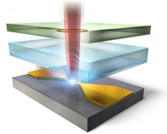
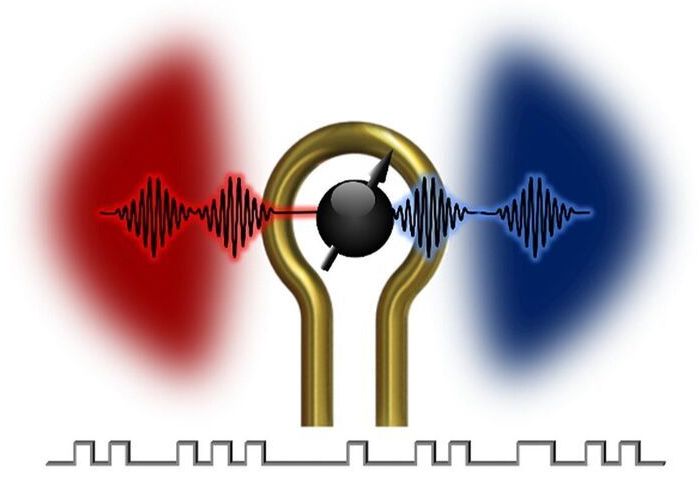
Scientists at the U.S. Department of Energy’s (DOE) Argonne National Laboratory and the University of Chicago’s Pritzker School of Molecular Engineering have devised a unique means of achieving effective gate operation with a form of processing called electromagnonics. Their pivotal discovery allows real-time control of information transfer between and magnons. And it could result in a new generation of classical electronic and quantum signal devices that can be used in various applications such as signal switching, low-power computing and quantum networking.

Microwave photons are forming the employed in, for example, wireless communications. Magnons are the particle-like representatives of “spin waves.” That is, wave-like disturbances in an ordered array of microscopically aligned spins that occur in certain magnetic materials.
The smaller transistors get, the more expensive they get, and similarly, the harder it becomes for foundries to compete at the cutting edge. We’ve been seeing this since the introduction of TSMC and Samsung’s 7nm node (comparable to Intel’s 10nm process). Global Foundries was the first to drop out of the race, and Intel has been stuck on its 14nm node for nearly seven years (although the chipmaker is trying to make a comeback). Samsung is the third major foundry struggling to keep up with TSMC in the race to make the smallest transistors.

Samsung’s 10nm and 7nm nodes were both on par with TSMC’s, at least in terms of transistor density, packing 0.52 and 0.95 million transistors per square mm. Meanwhile, Intel’s 10nm node was denser than both, with a density of 1.06 million per square mm. Starting with the 5nm node, Samsung’s nodes have fallen behind. The Korean foundry’s 5nm node has a transistor density of 1.27 million (per mm2), compared to 1.73 million on TSMC’s 5nm and 1.8 million on Intel’s 7nm.

The deltas become even wider with the 3nm node, with Samsung expected to offer a density of just 1.7 million, compared to 2.9 million on TSMC’s 3nm (despite not using GAA), and 3 million on Intel’s 3nm. Samsung has continued to lose foundry customers, with both Qualcomm and MediaTek shifting to TSMC due to poor supply. It’s being reported that NVIDIA too will rely on TSMC’s 5nm for its next-gen GPUs, resulting in the loss of another major client for the former. At this rate, Samsung might just throw in the towel even before its 3nm node begins mass production.

In a medical first, researchers harnessed the brain waves of a paralyzed man unable to speak — and turned what he intended to say into sentences on a computer screen.

It will take years of additional research but the study, reported Wednesday, marks an important step toward one day restoring more natural communication for people who can’t talk because of injury or illness.

“Most of us take for granted how easily we communicate through speech,” said Dr. Edward Chang, a neurosurgeon at the University of California, San Francisco, who led the work. “It’s exciting to think we’re at the very beginning of a new chapter, a new field” to ease the devastation of patients who lost that ability.

Circa 2012 One day ice from could be transformed to metal the be transported anywhere even into space.


Researchers have combined high-powered computing and ‘chemical intuition’ to discover new phases of ice at extremely high pressures nonexistent on Earth, but probably abundant elsewhere in the solar system. (Jan. 16, 2012)

TSMC is mulling setting up more fabs overseas, apart from its exsiting facility in Nanjing, China and the one being built in the US. TSMC is looking at building new fabs in Japan and Germany for 28nm and 12/16nm chip output. Apple is keen on adopting miniLED backlighting for its devices, and is likely to add China-based Luxshare as a second supplier of SMT services for miniLED BLUs. Meanwhile, notebook component suppliers are turning cautious about building up inventory amid mixed signals about the notebook market’s outlook.

TSMC mulls 28nm, 12/16nm process capacity expansion overseas: TSMC will soon disclose plans to build additional 28nm and 12/16nm process fabrication lines at new fabs, in addition to its Nanjing fab expansion, according to industry sources.

Luxshare to become second SMT service provider for miniLED backlighting for Apple: Taiwan Surface Mounting Technology (SMT) is currently the only provider of SMT services for Apple’s miniLED backlighting applications, but China-based Luxshare Precision Industry is expected to become a second provider in fourth-quarter 2021 at the earliest, according to industry sources.

Intel wants in on this, and hopes to expand its presence on the continent. It hopes to build in Europe at least one factory for manufacturing and another for advanced packaging, Greg Slater, VP of global regulatory affairs, told the Financial Times over the weekend. France, Germany, Belgium, and the Netherlands are being considered as hosts for these facilities, and Intel is expected to name locations by the end of the year.

Chipzilla is, we’re told, prepared to blow as much as $20bn on these factories over the next decade, with an eye on building up to eight fabs on a 1000-acre site somewhere with the necessary infrastructure around it. Intel teased it could spend up to $100bn during the lifetime of these Euro plants.

“We are well placed to make this an ecosystem-wide project, not just a couple of isolated paths in one member state,” Slater said. “We do believe that this is a project that will benefit Europe at large.”

Scientists from the Division of Physics at the University of Tsukuba used the quantum effect called ‘spin-locking’ to significantly enhance the resolution when performing radio-frequency imaging of nitrogen-vacancy defects in diamond. This work may lead to faster and more accurate material analysis, as well as a path towards practical quantum computers.

Nitrogen-vacancy (NV) centers have long been studied for their potential use in quantum computers. A NV center is a type of defect in the lattice of a diamond, in which two adjacent carbon atoms have been replaced with a nitrogen atom and a void. This leaves an unpaired electron, which can be detected using radio-frequency waves, because its probability of emitting a photon depends on its . However, the of radio wave detection using conventional radio-frequency techniques has remained less than optimal.

Now, researchers at the University of Tsukuba have pushed the resolution to its limit by employing a technique called ‘spin-locking’. Microwave pulses are used to put the electron’s spin in a quantum superposition of up and down simultaneously. Then, a driving electromagnetic field causes the direction of the spin to precess around, like a wobbling top. The end result is an electron spin that is shielded from random noise but strongly coupled to the detection equipment. “Spin-locking ensures high accuracy and sensitivity of the electromagnetic field imaging,” first author Professor Shintaro Nomura explains. Due to the high density of NV centers in the diamond samples used, the collective signal they produced could be easily picked up with this method. This permitted the sensing of collections of NV centers at the micrometer scale.

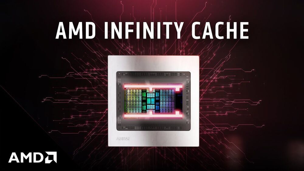
Infinity Cache is one of the headline features found in AMD’s RDNA 2 – the GPU architecture behind the next generation of gaming graphics, including the PS5, the Xbox Series X and, of course, AMD’s own Radeon RX 6000 graphics cards. But, what is Infinity Cache?

Read on to learn more about Infinity Cache, how it works and where you can find it.

Infinity Cache is an all-new cache level AMD says will improve the efficiency and performance of its RDNA 2 architecture during 4K and 1440p gaming.

Early in its history, computing was dominated by time-sharing systems. These systems were powerful machines (for their time, at least) that multiple users connected to in order to perform computing tasks. To an extent, quantum computing has repeated this history, with companies like Honeywell, IBM, and Rigetti making their machines available to users via cloud services. Companies pay based on the amount of time they spend executing algorithms on the hardware.

For the most part, time-sharing works out well, saving companies the expenses involved in maintaining the machine and its associated hardware, which often includes a system that chills the processor down to nearly absolute zero. But there are several customers—companies developing support hardware, academic researchers, etc.—for whom access to the actual hardware could be essential.

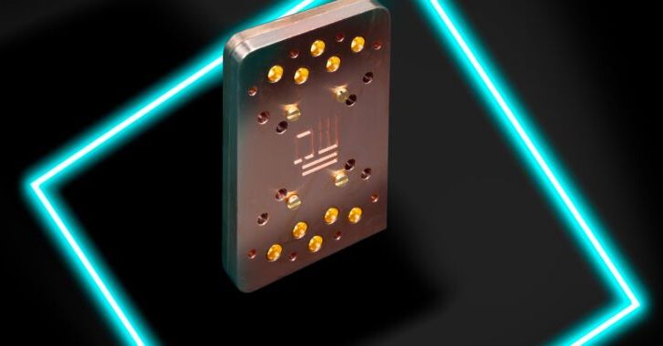
The fact that companies aren’t shipping out processors suggests that the market isn’t big enough to make production worthwhile. But a startup from the Netherlands is betting that the size of the market is about to change. On Monday, a company called QuantWare announced that it will start selling quantum processors based on transmons, superconducting loops of wire that form the basis of similar machines used by Google, IBM, and Rigetti.