Toggle light / dark theme

What is the ultimate goal of Artificial General Intelligence?

In this video series, the Galactic Public Archives takes bite-sized looks at a variety of terms, technologies, and ideas that are likely to be prominent in the future. Terms are regularly changing and being redefined with the passing of time. With constant breakthroughs and the development of new technology and other resources, we seek to define what these things are and how they will impact our future.

Follow us on social media:
Twitter / Facebook / Instagram

SEATTLE Boeing Co is looking ahead to a brave new world where jetliners fly without pilots and aims to test some of the technology next year, the world’s biggest plane maker said in a briefing ahead of the Paris Airshow.

The idea may seem far-fetched but with self-flying drones available for less than $1,000, “the basic building blocks of the technology clearly are available,” said Mike Sinnett, Boeing’s vice president of product development.

Jetliners can already take off, cruise and land using their onboard flight computers and the number of pilots on a standard passenger plane has dropped to two from three over the years.

Read more

One of Apple’s new announcements has tech experts excited for augmented reality. One chief executive calls it a “game-changer.”

Apple unveiled its new operating system for its iPhone and iPad products, the iOS 11, at the Apple Worldwide Developers Conference on Monday.

The system also introduces ARKit, a new framework for developers to more easily build apps that use augmented reality: the tech that allows devices to display computer-generated images over the real world.

Read more

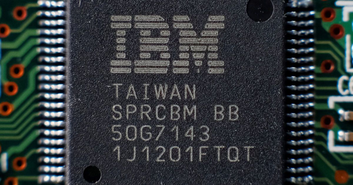
Who said Moore’s Law was dead? Certainly not IBM or its chip partners Globalfoundries and Samsung. The trio has developed a transistor manufacturing process that should pave the way for 5-nanometer chips. While the team etched the chip using the same extreme ultraviolet lithography (EUV) used for the breakthrough 7nm chip, it ditched the common FinFET (fin field effect) transistor design in favor of stacks of silicon nanosheets. The switch makes it possible to fine-tune individual circuits to maximize their performance as they’re crammed into an incredibly small space. How small? At 5nm, the group says it can squeeze 30 billion transistors into a chip the size of a fingernail (see below) — not bad when the 7nm chip held 20 billion transistors a couple of years ago.

IBM sees the technique helping its own cognitive computing efforts as well as the Internet of Things and other “data-intensive” tasks. However, it’s also painting a rosy picture for the future of mobile devices — it imagines phones having “two to three times” more battery life than current devices. That’s likely optimistic (phone makers tend to focus on speed over longevity), but it won’t be shocking if future hardware is both faster and wrings out a little more from every charge.

Just don’t expect to see real-world examples of this for a while. We haven’t even seen devices shipping with 7nm chips (they’re not expected until 2018 at the earliest), so it could easily be a couple of years or more before 5nm arrives. Still, that 5nm is even on the roadmap is important. Chip designers won’t have to reinvent the wheel to get meaningful improvements, and you won’t have to worry about device performance growing stale for at least the next few years.

Read more

Microsoft Research has published a technical paper reviewing their work with near-eye displays for virtual and augmented reality to project phase-only holograms.

The team built a holographic projector that displayed a series of sub-holograms, which allowed the hologram to display variable depths of focused light. The projector was then combined with a series of eyepieces to achieve the displays.

With their prototype display, the team was able to achieve high-quality holographic images. By processing holograms in the GPU, the team rendered 3D models in real time with depth-of-field.

Read more

IBM, in partnership with Samsung and GlobalFoundries (which manufactures chips for Qualcomm and AMD, among others), has developed a process for building 5nm chips. Two years ago IBM unveiled a 7nm process, and Samsung will likely ship 7nm chips next year, but today’s announcement sounds like an even more important breakthrough in chip design.

Read more

Today, Apple announced a brand-new tier of its all-in-one desktop called the iMac Pro. The new product, unveiled onstage at the company’s Worldwide Developers Conference in San Jose, California, is supposed to be a “the most powerful Mac ever,” according to the company. In other words, this computer is going to replace the painfully outdated and woefully mismanaged Mac Pro line, at least for the foreseeable future. The iMac Pro will start shipping this December starting at $4,999, Apple confirmed.

Apple says the computer will ship with an 8-core Xeon processor, with configurations that scale up to an 18-core Xeon processor, 5K display, and an all-new AMD Radeon Vega GPU. You’ll also be able to shell out for up to 16GB of VRAM, up to 128GB of data corruption-protecting ECC RAM, and up to 4TB for SSD storage. There’s a whole bunch of other upgrades in there. Check out the full list Apple shared in its presentation below:

Read more

IBM, its Research Alliance partners Globalfoundries and Samsung, and equipment suppliers have developed an industry-first process to build silicon nanosheet transistors that will enable 5 nanometer (nm) chips. The details of the process will be presented at the 2017 Symposia on VLSI Technology and Circuits conference in Kyoto, Japan. In less than two years since developing a 7nm test node chip with 20 billion transistors, scientists have paved the way for 30 billion switches on a fingernail-sized chip.

The resulting increase in performance will help accelerate cognitive computing, the Internet of Things (IoT), and other data-intensive applications delivered in the cloud. The power savings could also mean that the batteries in smartphones and other mobile products could last two to three times longer than today’s devices, before needing to be charged.

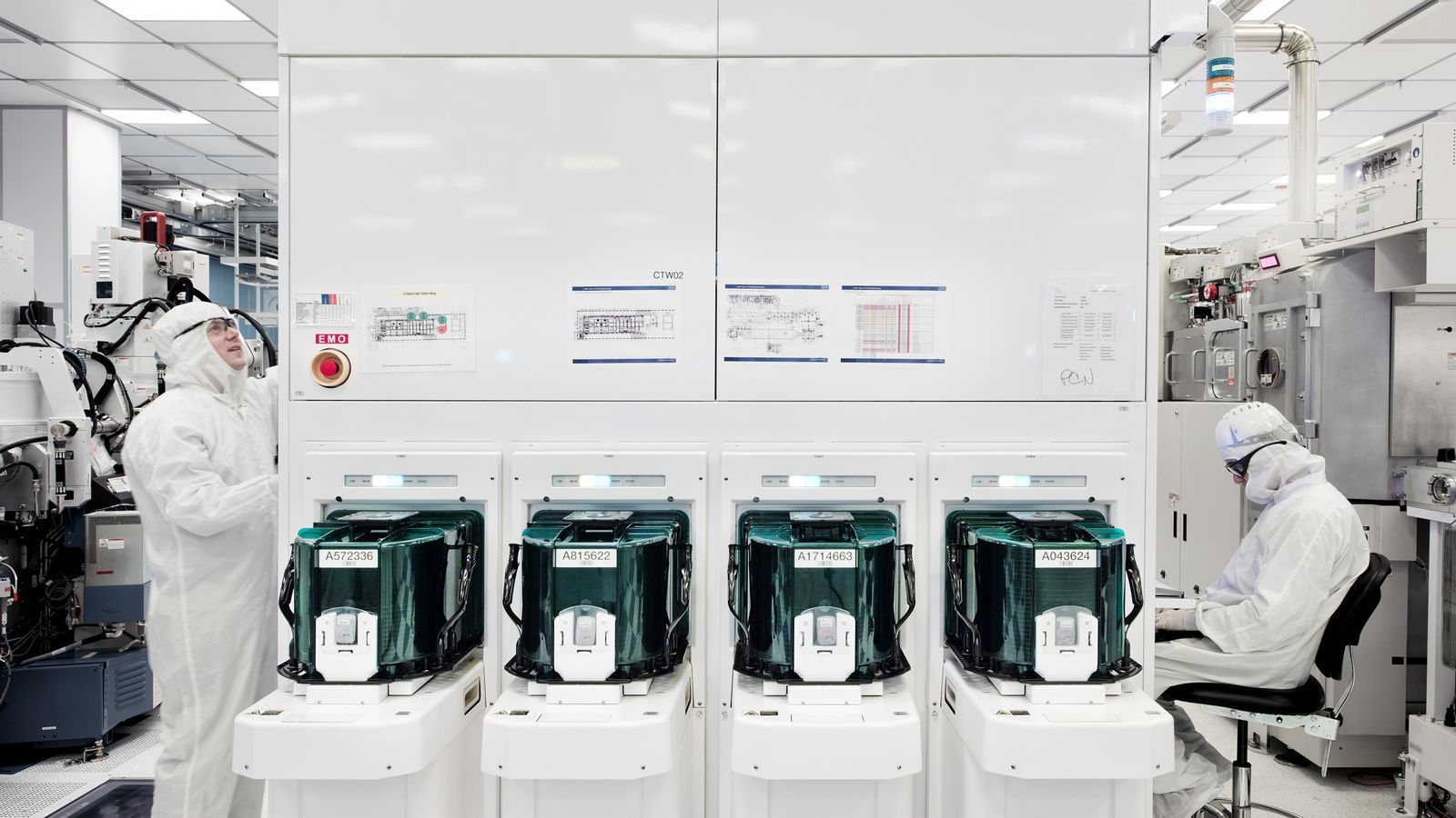
Scientists working as part of the IBM-led Research Alliance at the SUNY Polytechnic Institute Colleges of Nanoscale Science and Engineering’s NanoTech Complex in Albany, NY achieved the breakthrough by using stacks of silicon nanosheets as the device structure of the transistor, instead of the standard FinFET architecture, which is the blueprint for the semiconductor industry up through 7nm node technology.

Read more