Computer scientists have been searching for years for a type of problem that a quantum computer can solve but that any possible future classical computer cannot. Now they’ve found one.


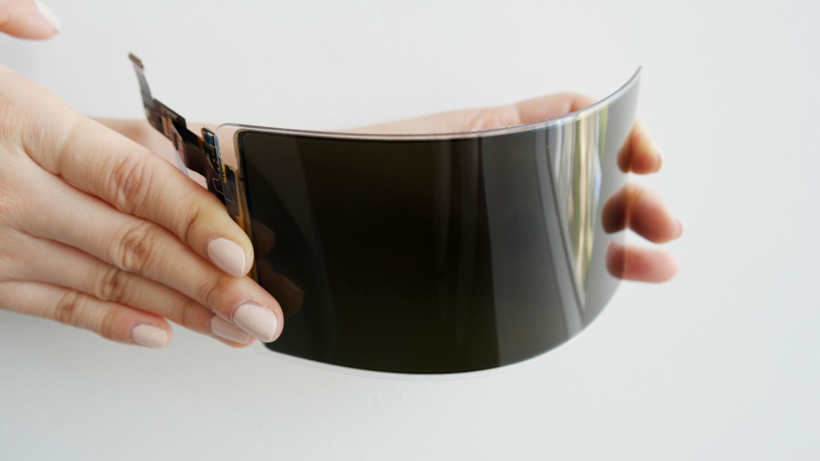
Samsung proudly announced today that its “unbreakable smartphone panel” has been certified by Underwriters Laboratories (UL). This means this ultra durable display is much closer to very profitable things like military and automotive contracts. But let’s be serious. Somebody’s gonna find a way to break this thing, and I hope it’s me.
The new display owes its anti-destructive tendencies to a couple of innovations. Samsung says that the OLED panel has “an unbreakable substrate.” (A substrate is basically the coating that holds the display’s organic material, cathodes, and diodes together.) Additionally, the Samsung display uses a flexible new type of plastic that won’t crack like glass. So you can supposedly drop it, smash it, and bend it without breaking the display.
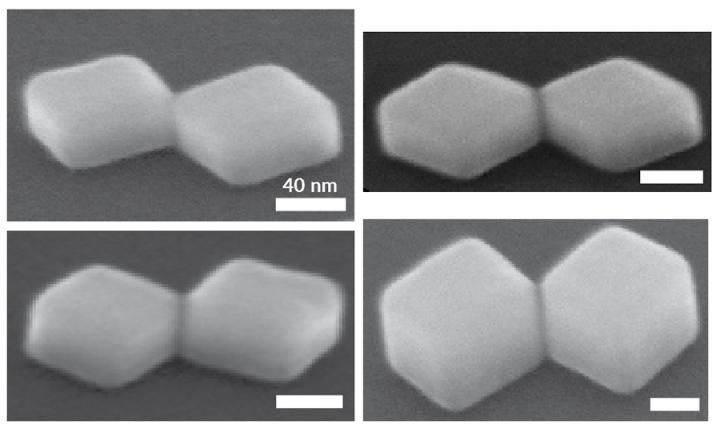
Using advanced fabrication techniques, engineers at the University of California San Diego have built a nanosized device out of silver crystals that can generate light by efficiently “tunneling” electrons through a tiny barrier. The work brings plasmonics research a step closer to realizing ultra-compact light sources for high-speed, optical data processing and other on-chip applications.
The work is published July 23 in Nature Photonics.
The device emits light by a quantum mechanical phenomenon known as inelastic electron tunneling. In this process, electrons move through a solid barrier that they cannot classically cross. And while crossing, the electrons lose some of their energy, creating either photons or phonons in the process.
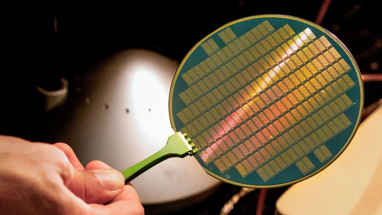
Silicon computer chips have been on a roll for half a century, getting ever more powerful. But the pace of innovation is slowing. Today the U.S. military’s Defense Advanced Research Projects Agency (DARPA) announced dozens of new grants totaling $75 million in a program that aims to reinvigorate the chip industry with basic research into new designs and materials, such as carbon nanotubes. Over the next few years, the DARPA program, which supports both academic and industry scientists, will grow to $300 million per year up to a total of $1.5 billion over 5 years.
“It’s a critical time to do this,” says Erica Fuchs, a computer science policy expert at Carnegie Mellon University in Pittsburgh, Pennsylvania.
In 1965, Intel co-founder Gordon Moore made the observation that would become his eponymous “law”: The number of transistors on chips was doubling every 2 years, a time frame later cut to every 18 months. But the gains from miniaturizing the chips are dwindling. Today, chip speeds are stuck in place, and each new generation of chips brings only a 30% improvement in energy efficiency, says Max Shulaker, an electrical engineer at the Massachusetts Institute of Technology in Cambridge. Fabricators are approaching physical limits of silicon, says Gregory Wright, a wireless communications expert at Nokia Bell Labs in Holmdel, New Jersey. Electrons are confined to patches of silicon just 100 atoms wide, he says, forcing complex designs that prevent electrons from leaking out and causing errors. “We’re running out of room,” he says.
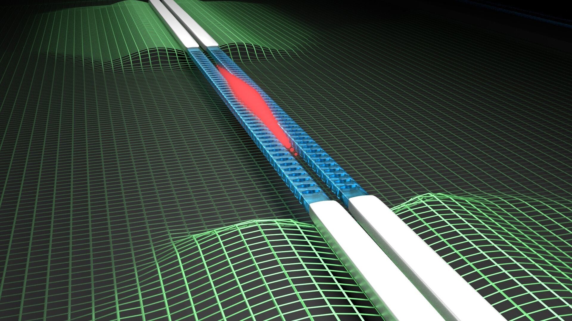
The Casimir force and superconductivity are two well-known quantum effects. These phenomena have been thoroughly studied separately, but what happens when these effects are combined in a single experiment? Now, Delft University of Technology have created a microchip on which two wires were placed in close proximity in order to measure the Casimir forces that act upon them when they become superconducting.
Is vacuum really empty? Quantum mechanics tells us that it’s actually swarming with particles. In the 1940s, Dutch physicists Hendrik Casimir and Dirk Polder predicted that when two objects are placed in very close proximity, about a thousandth of the diameter of a human hair, this sea of ‘vacuum particles’ pushes them together – a phenomenon known as the Casimir effect. This attractive force is present between all objects and even sets fundamental limits to how closely we can place components together on microchips.
Superconductivity is another well-known quantum phenomenon, also discovered by a Dutchman, Heike Kamerlingh Onnes, in the early 20th century. It describes how certain materials, such as aluminum or lead, allow electricity to flow through them without any resistance at cryogenic temperatures. Over the last 100 years, superconductors have revolutionized our understanding of physics and are responsible for magnetically levitated trains, MRI scans and even mobile phone stations.

Tomorrow it’s commercial tourism, space energy, space data centers, in-space manufacturing and resource exploration & utilization. Companies all over the world are creating incredible future technologies that will one day operate in deep space. But one question largely goes unanswered: how will they get there? We will take them.
Chemical and ion electrical propulsion have their limitations. We’re building breakthrough transportation technology to propel the next generation of space endeavors more efficiently, safely, and inexpensively than ever before.
