Toggle light / dark theme

When practical quantum computing finally arrives, it will have the power to crack the standard digital codes that safeguard online privacy and security for governments, corporations, and virtually everyone who uses the Internet. That’s why a U.S. government agency has challenged researchers to develop a new generation of quantum-resistant cryptographic algorithms.

Many experts don ’t expect a quantum computer capable of performing the complex calculations required to crack modern cryptography standards to become a reality within the next 10 years. But the U.S. National Institute of Standards and Technology (NIST) wants to stay ahead by getting new cryptographic standards ready by 2022. The agency is overseeing the second phase of its Post-Quantum Cryptography Standardization Process to narrow down the best candidates for quantum-resistant algorithms that can replace modern cryptography.

“Currently intractable computational problems that protect widely-deployed cryptosystems, such as RSA and Elliptic Curve-based schemes, are expected to become solvable,” says Rafael Misoczki, a cryptographer at the Intel Corporation and a member of two teams (named Bike and Classic McEliece) involved in the NIST process. “This means that quantum computers have the potential to eventually break most secure communications on the planet.”
An exotic physical phenomenon, involving optical waves, synthetic magnetic fields, and time reversal, has been directly observed for the first time, following decades of attempts. The new finding could lead to realizations of what are known as topological phases, and eventually to advances toward fault-tolerant quantum computers, the researchers say.

The new finding involves the non-Abelian Aharonov-Bohm Effect and is reported today in the journal Science by MIT graduate student Yi Yang, MIT visiting scholar Chao Peng (a professor at Peking University), MIT graduate student Di Zhu, Professor Hrvoje Buljan at University of Zagreb in Croatia, Francis Wright Davis Professor of Physics John Joannopoulos at MIT, Professor Bo Zhen at the University of Pennsylvania, and MIT professor of physics Marin Soljacic.

The finding relates to gauge fields, which describe transformations that particles undergo. Gauge fields fall into two classes, known as Abelian and non-Abelian. The Aharonov-Bohm Effect, named after the theorists who predicted it in 1959, confirmed that gauge fields—beyond being a pure mathematical aid—have physical consequences.

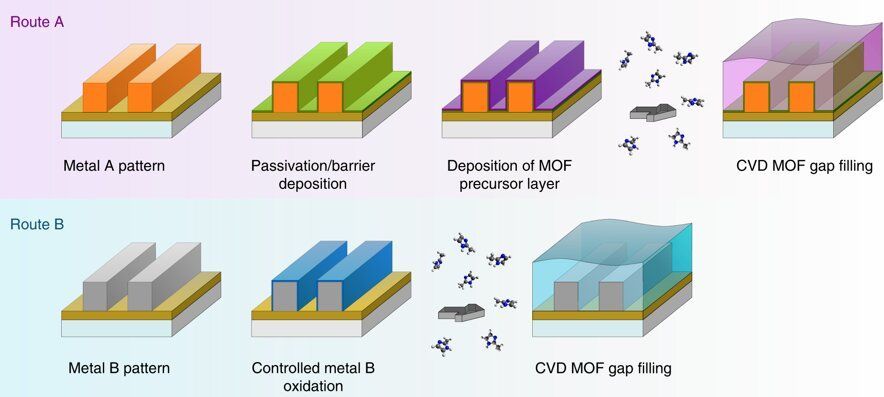
Researchers at KU Leuven and imec have successfully developed a new technique to insulate microchips. The technique uses metal-organic frameworks, a new type of materials consisting of structured nanopores. In the long term, this method can be used for the development of even smaller and more powerful chips that consume less energy. The team has received an ERC Proof of Concept grant to further their research.

Computer chips are getting increasingly smaller. That’s not new: Gordon Moore, one of the founders of chip manufacturer Intel, already predicted it in 1965. Moore’s law states that the number of transistors in a chip, or integrated circuit, doubles about every two years. This prognosis was later adjusted to 18 months, but the theory still stands. Chips are getting smaller and their processing power is increasing. Nowadays, a chip can have over a billion transistors.

But this continued reduction in size also brings with it a number of obstacles. The switches and wires are packed together so tightly that they generate more resistance. This, in turn, causes the chip to consume more energy to send signals. To have a well-functioning chip, you need an insulating substance that separates the wires from each other, and ensures that the electrical signals are not disrupted. However, that’s not an easy thing to achieve at the nanoscale level.

Light-emitting diodes made of indium gallium nitride provide better luminescence efficiency than many of the other materials used to create blue and green LEDs. But a big challenge of working with InGaN is its known dislocation density defects that make it difficult to understand its emission properties.

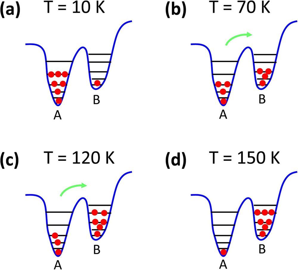
In the Journal of Applied Physics, researchers in China report an InGaN LED structure with high luminescence efficiency and what is believed to be the first direct observation of transition carriers between different localization states within InGaN. The localization states were confirmed by temperature-dependent photoluminescence and excitation power-dependent photoluminescence.

Localization states theory is commonly used to explain the high luminescence efficiency gained via the large number of dislocations within InGaN materials. Localization states are the energy minima states believed to exist within the InGaN quantum well region (discrete energy values), but a direct observation of localization states was elusive until now.

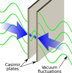
From the fictional universe of Stargate Atlantis and Marvel Comic’s Realm of Kings to NASA’s Eagleworks Propulsion laboratory, zero-point energy, also known as vacuum energy, is touted as a potentially limitless and ubiquitous source of energy, if one can only find the means to harness it. [1] Zero-point energy can be formulated in a few different ways, but in its most basic form, it is the minimal yet non-zero energy of a quantum mechanical system. In quantum field theory, zero-point energy can be considered by computing the expected energy of the zero photon mode. [2] In a system with no physical boundaries, the expected energy of the zero photon mode diverges! Yet, if this energy uniformly permeates all of space-time, it is not directly observable.

Conceptual Framework

For pedagogical reasons, we will consider the popular formulation of zero-point energy. The most interesting and relevant framework for zero-point energy can be understood from the quantum field theory for photons and electrons: quantum electrodynamics. Glossing over an exceptional amount of mathematical and conceptual background, the energy of a state in quantum field theory is computed as an expectation of a Hamiltonian„ which describes the energy of the state in terms of operators acting on wavefunctions. The final computation usually requires an integral over the allowed momenta of particles in the state.

“Over decades, both military and space programs all around the world have known the negative impact of radiation on semiconductor-based electronics,” says Meyya Meyyappan, Chief Scientist for Exploration Technology at the Center for Nanotechnology, at NASA’s Ames Research Center. What has changed with the push towards nanoscale feature sizes is that terrestrial levels of radiation can now also cause problems that had previously primarily concerned applications in space and defence. Packaging contaminants can cause alpha radiation that create rogue electron-hole pairs, and even the ambient terrestrial neutron flux at sea level – around 20 cm−2 h−1 – can have adverse implications for nanoscale devices.

Fortunately work to produce radiation-hardy electronics has been underway for some time at NASA, where space mission electronics are particularly prone to radiation exposure and cumbersome radiation shielding comes with a particularly costly load penalty. Vacuum electronics systems, the precursors to today’s silicon world, are actually immune to radiation damage. Alongside Jin-Woo Han and colleagues Myeong-Lok Seol, Dong-Il Moon and Gary Hunter at Ames and NASA’s Glenn Research Centre, Meyyappan has been working towards a renaissance of the old technology with a nano makeover.

In a recent Nature Electronics article, they report how with device structure innovations and a new material platform they can demonstrate nanoscale vacuum channel transistors that compete with solid-state system responses while proving impervious to radiation exposure.

Circa 2009


In just over a day, a powerful computer program accomplished a feat that took physicists centuries to complete: extrapolating the laws of motion from a pendulum’s swings.

Developed by Cornell researchers, the program deduced the natural laws without a shred of knowledge about physics or geometry.

The research is being heralded as a potential breakthrough for science in the Petabyte Age, where computers try to find regularities in massive datasets that are too big and complex for the human mind and its standard computational tools.

Truthfully, it has been some time since Moore’s law, the propensity for processors to double in transistor count every two years, has been entirely accurate. The fundamental properties of silicon are beginning to limit development and will significantly curtail future performance gains, yet with 50 years and billions invested, it seems preposterous that any ‘beyond-silicon’ technology could power the computers of tomorrow. And yet, Nano might do just that, by harnessing its ability to be designed and built like a regular silicon wafer, while using carbon to net theoretical triple performance at one-third the power.

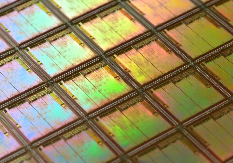
Nano began life much like all processors, a 150mm wafer with a pattern carved out of it by a regular chip fab. Dipped into a solution of carbon nanotubes bound together like microscopic spaghetti, it re-emerged with its semi-conductive carbon nanotubes stuck in the pattern of transistors and logic gates already etched on it. It then undergoes a process called ‘RINSE,’ removal of incubated nanotubes through selective exfoliation, by being coated with a polymer then dipped in a solvent. This has the effect of reducing the CNT layer to being just one tube, removing the large clumps of CNTs that stick together over 250 times more effectively than previous methods.

One of the challenges facing CNT processors has been difficulty in separating N-type and P-type transistors, which are “on” for 1 bit and “off” for 0 bit and the reverse, respectively. The difference is important for binary computing, and to perfect it, the researchers introduced ‘MIXED,’ metal interface engineering crossed with electrostatic doping. Occurring after RINSE, small platinum or titanium components are added to each transistor, then the wafer is coated in an oxide which acts as a sealant, improving performance. After that, Nano was just about done.