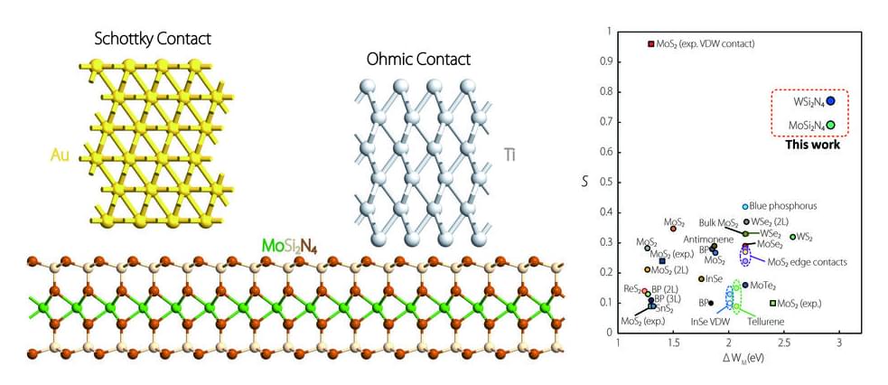
According to researchers from the Singapore University of Technology and Design (SUTD), a recently discovered family of two-dimensional (2D) semiconductors could pave the way for high-performance and energy-efficient electronics. Their findings, published in npj 2D Materials and Applications, may lead to the fabrication of semiconductor devices applicable in mainstream electronics and optoelectronics—and even potentially replace silicon-based device technology altogether.
In the quest of miniaturizing electronic devices, one well-known trend is Moore’s law, which describes how the number of components in the integrated circuits of computers doubles every two years. This trend is possible thanks to the ever-decreasing size of transistors, some of which are so small that millions of them can be crammed onto a chip the size of a fingernail. But as this trend continues, engineers are starting to grapple with the inherent material limitations of silicon-based device technology.
“Due to the quantum tunneling effect, shrinking a silicon-based transistor too small will lead to highly uncontrollable device behaviors,” said SUTD Assistant Professor Ang Yee Sin, who led the study. “People are now looking for new materials beyond the ‘silicon era’, and 2D semiconductors are a promising candidate.”
