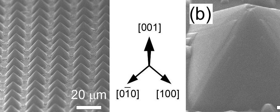
Ultra-small integrated circuits have revolutionized mobile phones, home appliances, cars, and other everyday technologies. To further miniaturize electronics and enable advanced functions, circuits must be reliably fabricated in three dimensions. Achieving ultrafine 3D shape control by etching into silicon is difficult, because even atomic-scale damage reduces device performance. Researchers at Nara Institute of Science and Technology (NAIST) have published a new study in Crystal Growth and Design in which they etched silicon to adopt the shape of atomically smooth pyramids. Coating these silicon pyramids with a thin layer of iron imparted magnetic properties that until now were only theoretical.
NAIST researcher and senior author of the study Ken Hattori is widely published in the field of atomically controlled nanotechnology. One focus of Hattori’s research is in improving the functionality of silicon-based technology.
“Silicon is the workhorse of modern electronics because it can act as a semiconductor or an insulator, and it’s an abundant element. However, future technological advances require atomically smooth device fabrication in three dimensions,” says Hattori.
