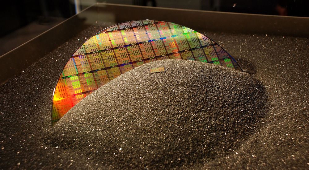
One of the ongoing questions these past few months has been why so many tech products have been so hard to buy. We’ve made repeated reference to known potential factors like COVID-19, economic disruptions, yield issues, and the impact of scalping bots, but there’s a new argument for what’s causing such general problems across so many markets: Insufficient investment in 200mm wafers.
Today, leading-edge silicon is invariably manufactured on 300mm wafers. Over the past few decades, manufacturers have introduced larger wafer sizes: 100mm, 150mm, 200mm, and 300mm have all been common standards at one time or another. In the PC enthusiast space, 300mm wafers have long been considered superior to 200mm wafers, because the larger wafer size reduces waste and typically improves the foundry’s output in terms of chips manufactured per day.
There aren’t that many commercial foundries still dedicated to 150mm or smaller wafer sizes, but a number of foundries still run 200mm fab lines. TSMC and Samsung both offer the node, as well as a number of second-tier foundries. GlobalFoundries has 200mm facilities, as do SMIC, UMC, TowerJazz, and SkyWater. A great many IoT and 5G chips are built on 200mm, as are some analog processors, MEMS devices, and RF solutions.
