Semiconductors are the basic building blocks of today’s digital, electronic age, providing us a multitude of devices that benefit our modern life, including computer, smartphones and other mobile devices. Improvements in semiconductor functionality and performance are likewise enabling next-generation applications of semiconductors for computing, sensing and energy conversion. Yet researchers have long struggled with limitations in our ability to fully understand the electronic charges inside semiconductor devices and advanced semiconductor materials, limiting our ability to drive further advances.
In a new study in the journal Nature, an IBM Research-led collaboration describes an exciting breakthrough in a 140-year-old mystery in physics—one that enables us to unlock the physical characteristics of semiconductors in much greater detail and aid in the development of new and improved semiconductor materials.
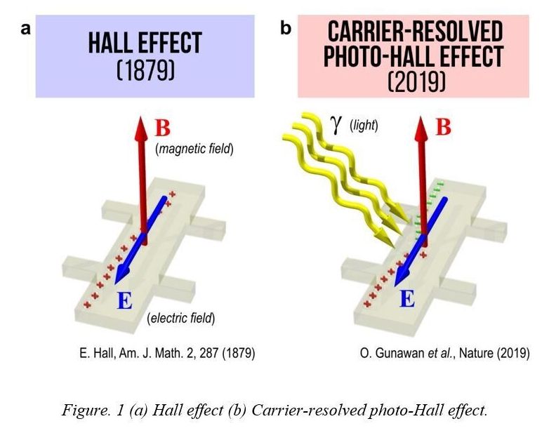
To truly understand the physics of semiconductors, we first need to know the fundamental properties of the charge carriers inside the materials, whether those particles are positive or negative, their speed under an applied electric field and how densely they are packed in the material. Physicist Edwin Hall found a way to determine those properties in 1879, when he discovered that a magnetic field will deflect the movement of electronic charges inside a conductor and that the amount of deflection can be measured as a voltage perpendicular to the flow of charge as shown in Fig. 1a. This voltage, known as the Hall voltage, unlocks essential information about the charge carriers in a semiconductor, including whether they are negative electrons or positive quasi-particles called “holes,” how fast they move in an electric field or their “mobility” (µ) and their density (n) inside the semiconductor.
