Toggle light / dark theme

Nice forum on QC Crystal Superconduction in Mar.


From March 8–10, 2017, an International Conference on Crystal Growth is to be held in Freiburg under the auspices of the German Association of Crystal Growth DGKK and the Swiss Society for Crystallography SGK-SSCR. The conference, jointly organized by the Fraunhofer Institute for Solar Energy Systems ISE, the Crystallography department of the Institute of Earth and Environmental Sciences at the University Freiburg and the University of Geneva, is to be held in the seminar rooms of the Chemistry Faculty of the University of Freiburg. Furthermore, the Young DGKK will hold a seminar for young scientists at Fraunhofer ISE on March 7, 2017.

“Whether for mobile communication, computers or LEDs, crystalline materials are key components of our modern lifestyle,” says Dr. Stephan Riepe, group head in the Department of Silicon Materials at Fraunhofer ISE. “Crystal growth has a long tradition and today is still far from becoming obsolete. Materials with special crystalline structure are being developed for applications in high-temperature superconductors through to low-loss power transmission. Artificial diamonds are a favorite choice for building quantum computers. At the conference, the production of silicon, III-V semiconductors and most currently perovskite layers for cost-effective high efficiency tandem solar cells will also be discussed.”

In Freiburg, a close cooperation exists between the Fraunhofer Institutes and the University of Freiburg. For example, at Fraunhofer ISE a doctoral thesis of the University of Freiburg was carried out which investigated how impurities can be minimized during multicrystalline silicon production. In the production process, liquid silicon is melted in a quartz crucible and subsequently solidified. Similar to flour’s function when sprinkled in a baking form, silicon nitride powder acts as a separating agent between the crucible and the silicon. Here the aim is to reduce impurities on the scale of parts per billion, or ppb, to achieve the highest solar cell efficiencies. On a regular basis, student and doctoral degree theses are carried out to address such questions.

Read more

New Graphene based flash memory card coming.


Dotz Nano (ASX: DTZ) has successfully completed a proof of concept research study into the use of Graphene Quantum Dots (GQDs) in flash memory devices with the Kyung Hee University in South Korea.

GQDs are being developed for use in various applications including medical imaging, sensing, consumer electronics, energy storage, solar cells and computer storage.

Dotz Nano is in advanced negotiations to sign a full licensing agreement with Kyung Hee University related to this technology.

Read more

In what could be called a classic “Eureka” moment, UC Santa Barbara materials researchers have discovered a simple yet effective method for mastering the electrical properties of polymer semiconductors. The elegant technique allows for the efficient design and manufacture of organic circuitry (the type found in flexible displays and solar cells, for instance) of varying complexity while using the same semiconductor material throughout.

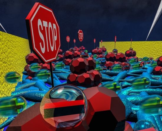
“It’s a different strategy by which you can take a material and change its properties,” said Guillermo Bazan, a professor of chemistry and at UCSB. With the addition of fullerene or copper tetrabenzoporphyrin (CuBP) molecules in strategic places, the charge carriers in semiconducting materials—negative electrons and positive “holes”—may be controlled and inverted for better device performance as well as economical manufacture. The discovery is published in a pair of papers that appear in the journals Advanced Functional Materials and Advanced Electronic Materials.

In the realm of , device functionality depends on the movement of the appropriate charge carriers across the material. There have been many advances in the synthesis of high-mobility, high-performance materials, said lead author Michael Ford, graduate student in materials, but the fine control of the electrons and holes is what will allow these sophisticated polymers to reach their full potential.

Read more

Graphene cooking oil?


In Brief

  • Researchers have discovered a way to make soybean oil into the super-strong material graphene. The material has a wide variety of potential uses and can revolutionize electronics.
  • The material could be used to make cell phone batteries last 25 percent longer, make more effective solar cells, and even filter fuel out of air.

Researchers have found a way to turn cheap, everyday cooking oil into the wonder material graphene – a technique that could greatly reduce the cost of making the much-touted nanomaterial.

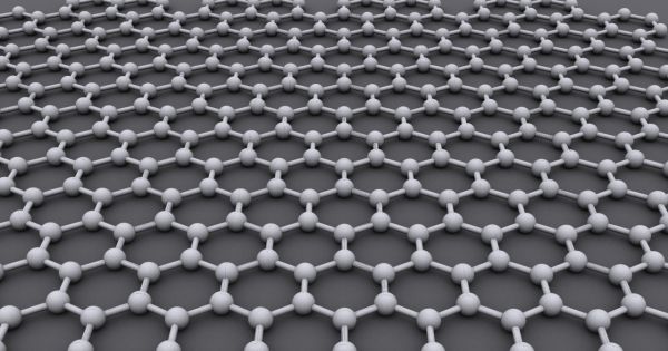
Graphene is a single sheet of carbon atoms with incredible properties – it’s 200 times stronger than steel, harder than diamond, and incredibly flexible. Under certain conditions, it can even be turned into a superconductor that carries electricity with zero resistance.

Read more

When it comes to obtaining new energy, solar energy now costs less than fossil fuels, according to a report by the World Economic Forum (WEF). Data from Bloomberg New Energy Finance (BNEF) also show decreased prices, with the mean price of solar power in about 60 countries dropping to $1.65 million per megawatt, closely followed by wind at $1.66 million per megawatt.

Michael Drexler, Head of Long Term Investing, Infrastructure and Development at the World Economic Forum, found the downturn in prices to be an encouraging sign.

“Renewable energy has reached a tipping point—it now constitutes the best chance to reverse global warming. Solar and wind have just become very competitive, and costs continue to fall. It is not only a commercially viable option, but an outright compelling investment opportunity with long-term, stable, inflation-protected returns.”

Read more

Solar cells convert light into electricity. While the sun is one source of light, the burning of natural resources like oil and natural gas can also be harnessed.

However, solar cells do not convert all light to power equally, which has inspired a joint industry-academia effort to develop a potentially game-changing solution.

“Current solar cells are not good at converting visible light to electrical power. The best efficiency is only around 20%,” explains Kyoto University’s Takashi Asano, who uses optical technologies to improve energy production.

Read more

Harvesting light.


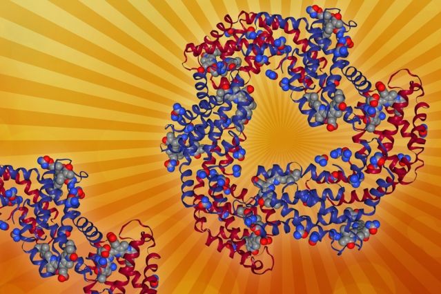
Plants and other photosynthetic organisms use a wide variety of pigments to absorb different wavelengths of light. MIT researchers have now developed a theoretical model to predict the spectrum of light absorbed by aggregates of these pigments, based on their structure.

The new model could help guide scientists in designing new types of solar cells made of organic materials that efficiently capture light and funnel the light-induced excitation, according to the researchers.

“Understanding the sensitive interplay between the self-assembled pigment superstructure and its electronic, optical, and transport properties is highly desirable for the synthesis of new materials and the design and operation of organic -based devices,” says Aurelia Chenu, an MIT postdoc and the lead author of the study, which appeared in Physical Review Letters on Jan. 3.

Read more

Plants and other photosynthetic organisms use a wide variety of pigments to absorb different wavelengths of light. MIT researchers have now developed a theoretical model to predict the spectrum of light absorbed by aggregates of these pigments, based on their structure.

The could help guide scientists in designing new types of solar cells made of organic materials that efficiently capture and funnel the light-induced excitation, according to the researchers.

“Understanding the sensitive interplay between the self-assembled pigment superstructure and its electronic, optical, and transport properties is highly desirable for the synthesis of new materials and the design and operation of organic-based devices,” says Aurelia Chenu, an MIT postdoc and the lead author of the study, which appeared in Physical Review Letters on Jan. 3.

Read more

In the past decade, two-dimensional, 2D, materials have captured the fascination of a steadily increasing number of scientists. These materials, whose defining feature is having a thickness of only one to very few atoms, can be made of a variety of different elements or combinations thereof. Scientists’ enchantment with 2D materials began with Andre Geim and Konstantin Novoselov’s Nobel Prize winning experiment: creating a 2D material using a lump of graphite and common adhesive tape. This ingeniously simple experiment yielded an incredible material: graphene. This ultra-light material is roughly 200 times stronger than steel and is a superb conductor. Once scientists discovered that graphene had more impressive properties than its bulk component graphite, they decided to investigate other 2D materials to see if this was a universal property.

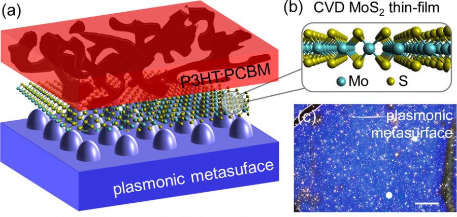
Christopher Petoukhoff, a Rutgers University graduate student working in the Femtosecond Spectroscopy Unit at the Okinawa Institute of Science and Technology Graduate University (OIST), studies a 2D material, made of molybdenum disulfide (MoS2). His research focuses on the 2D material’s optoelectronic applications, or how the material can detect and absorb light. Optoelectronics are ubiquitous in today’s world, from the photodetectors in automatic doors and hand dryers, to solar cells, to LED lights, but as anyone who has stood in front of an automatic sink desperately waving their hands around to get it to work will tell you, there is plenty of room for improvement. The 2D MoS2 is particularly interesting for use in photodetectors because of its capability of absorbing the same amount of light as 50nm of the currently used silicon-based technologies, while being 70 times thinner.

Petoukhoff, under the supervision of Professor Keshav Dani, seeks to improve optoelectronic devices by adding a 2D layer of MoS2 to an organic semiconductor, which has similar absorption strengths as MoS2. The theory behind using both materials is that the interaction between the MoS2 layer and the organic semiconductor should lead to efficient charge transfer. Petoukhoff’s research, published in ACS Nano, demonstrates for the first time that charge transfer between these two layers occurs at an ultra-fast timescale, on the order of less than 100 femtoseconds, or one tenth of one millionth of one millionth of a second.

Read more