Toggle light / dark theme

A team of physicists from the University of Konstanz and Ludwig-Maximilians-Universität München in Germany have achieved attosecond time resolution in a transmission electron microscope by combining it with a continuous-wave laser—offering new insights into light-matter interactions.

Electron microscopes provide deep insight into the smallest details of matter and can reveal, for example, the atomic configuration of materials, the structure of proteins or the shape of virus particles. However, most materials in nature are not static and rather interact, move and reshape all the time. One of the most common phenomena is the interaction between and matter, which is ubiquitous in plants as well as in , solar cells, displays or lasers. These interactions—which are defined by electrons being moved around by the field cycles of a light wave—happen at ultrafast time scales of femtoseconds (10-15 seconds) or even attoseconds (10-18 seconds, a billionth of a billionth of a second). While ultrafast electron microscopy can provide some insight into femtosecond processes, it has not been possible, until now, to visualize the reaction dynamics of light and matter occurring at attosecond speeds.

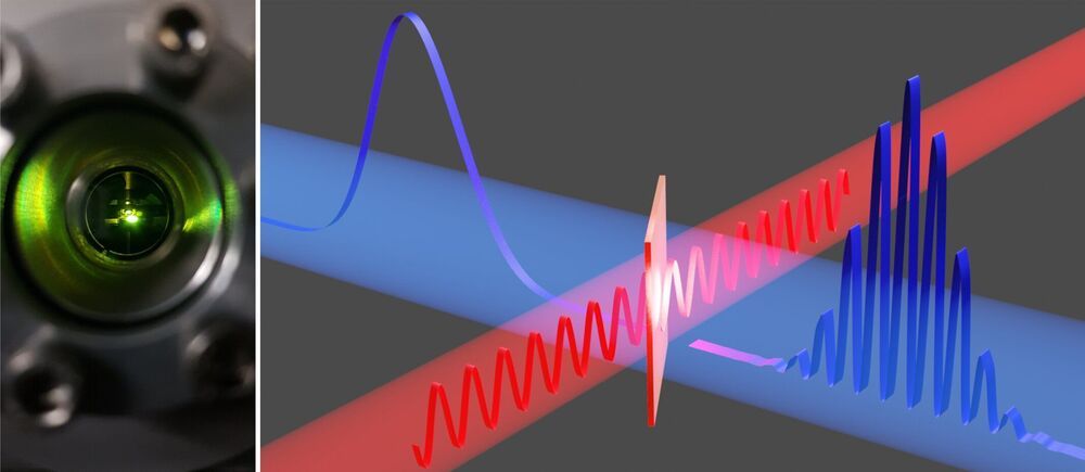
Now, a team of physicists from the University of Konstanz and Ludwig-Maximilians-Universität München have succeeded in combining a with a continuous-wave laser to create a prototypical attosecond electron (A-TEM). The results are reported in the latest issue of Science Advances.
Nanographene is a material that could radically improve solar cells, fuel cells, LEDs and more. Typically, the synthesis of this material has been imprecise and difficult to control. For the first time, researchers have discovered a simple way to gain precise control over the fabrication of nanographene. In doing so, they have shed light on the previously unclear chemical processes involved in nanographene production.

Graphene, one-atom-thick sheets of carbon molecules, could revolutionize future technology. Units of graphene are known as ; these are tailored to specific functions, and as such, their fabrication process is more complicated than that of generic graphene. Nanographene is made by selectively removing from organic molecules of carbon and hydrogen, a process called dehydrogenation.

“Dehydrogenation takes place on a such as that of silver, gold or copper, which acts as a catalyst, a material that enables or speeds up a reaction,” said Assistant Professor Akitoshi Shiotari from the Department of Advanced Materials Science. “However, this surface is large relative to the target organic molecules. This contributes to the difficulty in crafting specific nanographene formations. We needed a better understanding of the catalytic process and a more precise way to control it.”

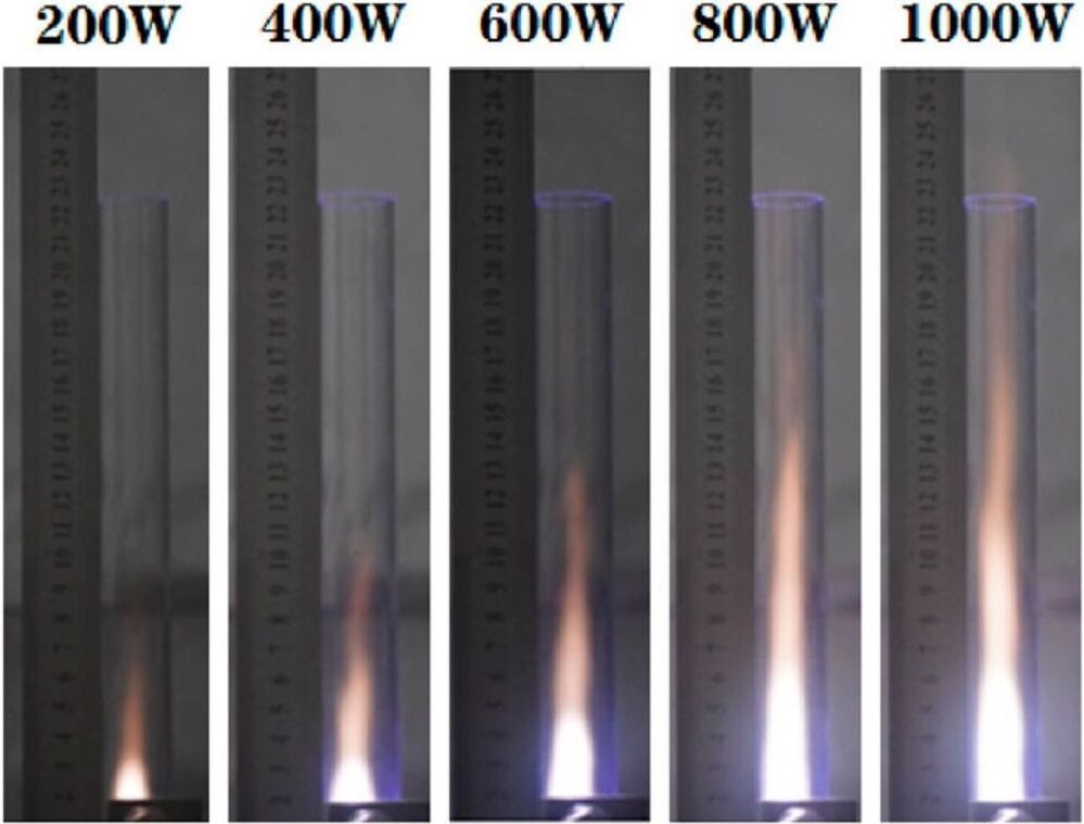
A Chinese team has demonstrated a prototype of a microwave plasma thruster capable of working in the Earth’s atmosphere and producing thrust with an efficiency comparable to the jet engines you’d find on modern airliners – under laboratory conditions.

Plasma thrusters are already operational on spacecraft as a means of solar-electric locomotion, using xenon plasma, but such things are no use in the Earth’s atmosphere, as accelerated xenon ions lose most of their thrust force to friction against the air. Not to mention, they only make a small amount of thrust in the first place.

This design, conceived and built by a team at the Institute of Technical Sciences at Wuhan University, uses only air and electricity, and appears to produce an impressive push that may see it become relevant to electric aircraft applications.

It seems solar power is really benefiting these chicken farmers from Australia. It allows them to slash their electricity bill.


This 10-million-bird chicken farm has slashed its power bill and reduced its CO2 emissions by 1,500 tonnes after installing one of agriculture’s most extensive solar and battery systems.

This is one of four blogs in a series examining current challenges and opportunities for recycling of clean energy technologies. Please see the introductory post, as well as other entries on solar panels and wind turbines.


us department of energy[ caption] courtesy union concerned scientists. by james gignac, lead midwest energy analyst this is one four blogs in a series examining current challenges and opportunities for recycling clean technologies. please see the introductory post, as well other entries on solar panels and wind turbines. special thanks to jessica garcia, ucs’s=

Well, at least they’re having fun with it.


Most sun oriented homesteads adjust their sunlight based exhibits in lines and segments to shape a matrix.

Another sun based force plant in Datong, China, be that as it may, chose to have some good times with its structure. China Dealers New Vitality Gathering, one of the nation’s biggest clean vitality administrators, fabricated a 248-section of land sun powered ranch looking like a mammoth panda.

Ultra high-res displays for gadgets and tv sets may be coming. 😃


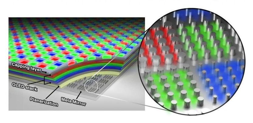
By expanding on existing designs for electrodes of ultra-thin solar panels, Stanford researchers and collaborators in Korea have developed a new architecture for OLED—organic light-emitting diode—displays that could enable televisions, smartphones and virtual or augmented reality devices with resolutions of up to 10,000 pixels per inch (PPI). (For comparison, the resolutions of new smartphones are around 400 to 500 PPI.)

Such high-pixel-density displays will be able to provide stunning images with true-to-life detail—something that will be even more important for headset displays designed to sit just centimeters from our faces.

The advance is based on research by Stanford University materials scientist Mark Brongersma in collaboration with the Samsung Advanced Institute of Technology (SAIT). Brongersma was initially put on this research path because he wanted to create an ultra-thin solar panel design.

Netherlands-based technology companies Avy and Wattlab have conducted the first test flight of a drone prototype that is planned to be used in medical projects in Africa.


Wattlab, a Dutch clean-tech start-up founded by Sweden-based power utility Vattenfall and Delft University of Technology, and Netherlands-based drone manufacturer Avy have announced that a drone equipped with special solar foils produced by Wattlab has successfully performed its first test flight.

“The solar-powered prototype is designed to be used for urgent medical transportation, emergency services, and nature conservation,” the two companies stated, adding that the solar films were installed on the wings while maintaining aerodynamics and without increasing significantly the weight. “The solar technology developed in this project is fully integrated into the wing shape and adds no extra weight,” explained Bo Salet, founder of Wattlab.

In the future, the two tech companies are planning to reduce the wings’ weight, increase their surface, and deploy more solar films. “Solar cells with a higher efficiency will be tested in the coming month,” they further explained.

“We’re not moving heat from the surface to the atmosphere. We’re just dumping it all out into the universe, which is an infinite heat sink,” said Xiangyu Li, a postdoctoral researcher at the Massachusetts Institute of Technology who worked on this project as a Ph.D. student in Ruan’s lab.


WEST LAFAYETTE, Ind. — What if paint could cool off a building enough to not need air conditioning?

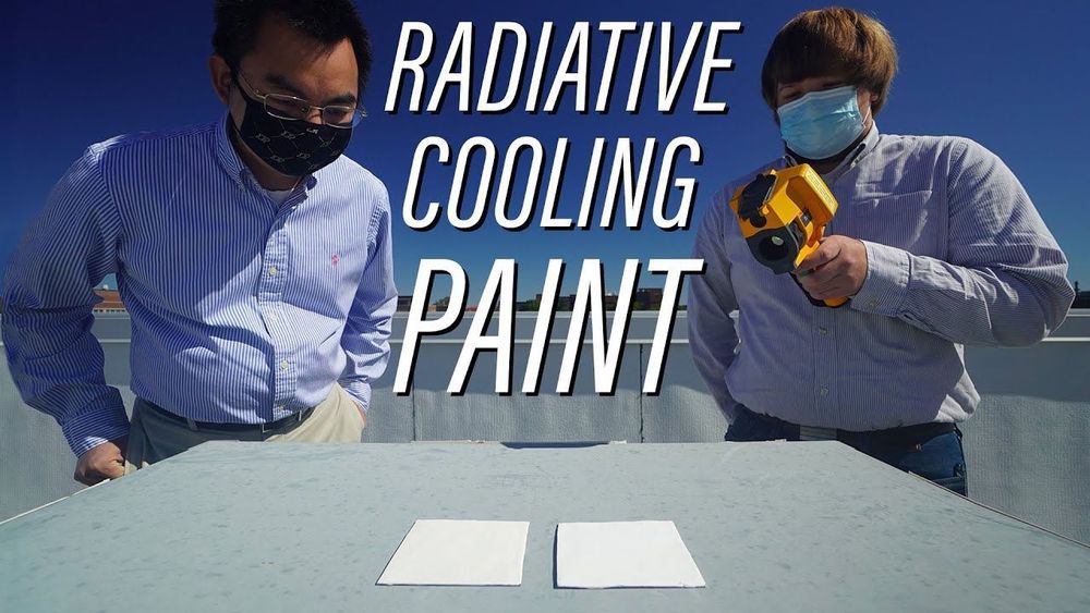
Purdue University engineers have created white paint that can keep surfaces up to 18 degrees Fahrenheit cooler than their ambient surroundings – almost like a refrigerator does, but without consuming energy.

According to the researchers, the paint would replace the need for air conditioning by absorbing nearly no solar energy and sending heat away from the building. Without the building heating up, air conditioning wouldn’t have to kick on.