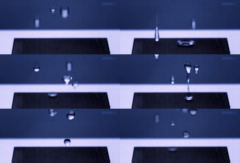
Using laser to build nanostructures on metal; and watch water bounce off the nanostructure coating
https://m.facebook.com/story.php?story_fbid=880054655441835&id=778276028953032

Using laser to build nanostructures on metal; and watch water bounce off the nanostructure coating
https://m.facebook.com/story.php?story_fbid=880054655441835&id=778276028953032
What would be really cool is have a “Computer Screen in a Can”; take your polymer spray and instantly create a screen on a table, a window, suitcase, etc. with your “Computer Screen in a Can”; U Can! I can just imagine the infomercials. On a more serious note — NW Univ has developed a new Hybrid Polymer which is going to expand the capabilities of polymer into so many areas in medicine, to manufacturing, electronics, self reparing material & devices, etc.
http://www.compositesworld.com/news/northwestern-university-researchers-develop-a-hybrid-polymer
A completely new hybrid polymer has been developed by Northwestern University (Evanston, IL) researchers.
“We have created a surprising new polymer with nano-sized compartments that can be removed and chemically regenerated multiple times,” said materials scientist Samuel Stupp, the senior author of the study and director of Northwestern’s Simpson Querrey Institute for BioNanotechnology. The study was published in the Jan. 29 issue of Science.
“Some of the nanoscale compartments contain rigid conventional polymers, but others contain the so- called supramolecular polymers, which can respond rapidly to stimuli, be delivered to the environment and then be easily regenerated again in the same locations. The supramolecular soft compartments could be animated to generate polymers with the functions we see in living things,” he said.
Interesting — I need to check in this one a little more.
Abstract: Researchers from Iran and Malaysia designed a nanostructure based on carbon nanotubes with antibacterial properties to be used in public places, specially hospitals and clinics.

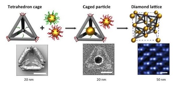
Building building diamond lattices through DNA.
Using bundled strands of DNA to build Tinkertoy-like tetrahedral cages, scientists at the U.S. Department of Energy’s Brookhaven National Laboratory have devised a way to trap and arrange nanoparticles in a way that mimics the crystalline structure of diamond. The achievement of this complex yet elegant arrangement, as described in a paper published February 5, 2016, in Science, may open a path to new materials that take advantage of the optical and mechanical properties of this crystalline structure for applications such as optical transistors, color-changing materials, and lightweight yet tough materials.
“We solved a 25-year challenge in building diamond lattices in a rational way via self-assembly,” said Oleg Gang, a physicist who led this research at the Center for Functional Nanomaterials (CFN) at Brookhaven Lab in collaboration with scientists from Stony Brook University, Wesleyan University, and Nagoya University in Japan.
The scientists employed a technique developed by Gang that uses fabricated DNA as a building material to organize nanoparticles into 3D spatial arrangements. They used ropelike bundles of double-helix DNA to create rigid, three-dimensional frames, and added dangling bits of single-stranded DNA to bind particles coated with complementary DNA strands.

Wonderful article on Nanotechnology and cancer with NCI’s Dr. Piotr Grodzinski. NCI established NCI’s with NCI’s Dr. Piotr Grodzinski. The article was published by declara.
Learn about Opportunities in Cancer Nanotechnology: A Conversation with NCI’s Dr. Piotr Grodzinski. Declara makes it easy to discover, share and organize knowledge. We empower individuals, organizations and countries to develop the knowledge needed to solve big problems.

UT RESEARCHERS DEVELOP ®EVOLUTIONARY CIRCUITS
Researchers of the MESA+ Institute for Nanotechnology and the CTIT Institute for ICT Research at the University of Twente in The Netherlands have demonstrated working electronic circuits that have been produced in a radically new way, using methods that resemble Darwinian evolution. The size of these circuits is comparable to the size of their conventional counterparts, but they are much closer to natural networks like the human brain. The findings promise a new generation of powerful, energy-efficient electronics, and have been published in the leading British journal Nature Nanotechnology.
One of the greatest successes of the 20th century has been the development of digital computers. During the last decades these computers have become more and more powerful by integrating ever smaller components on silicon chips. However, it is becoming increasingly hard and extremely expensive to continue this miniaturisation. Current transistors consist of only a handful of atoms. It is a major challenge to produce chips in which the millions of transistors have the same characteristics, and thus to make the chips operate properly. Another drawback is that their energy consumption is reaching unacceptable levels. It is obvious that one has to look for alternative directions, and it is interesting to see what we can learn from nature. Natural evolution has led to powerful ‘computers’ like the human brain, which can solve complex problems in an energy-efficient way. Nature exploits complex networks that can execute many tasks in parallel.

Transport Quantum bits via superconducting nanowires. Definite step forward in information transmittal capabilities.
Although 74 picoseconds may not sound like much — a picosecond is a trillionth of a second — it is a big deal in the quantum world, where light particles, or photons, can carry valuable information. In this case it means that much less “jitter,” or uncertainty in the arrival time of a photon. Less jitter means that photons can be spaced more closely together but still be correctly detected. This enables communications at a higher bit rate, with more information transmitted in the same period.
Every little bit helps when trying to receive faint signals reliably. It helped, for example, in NIST’s recent quantum teleportation record and difficult tests of physics theories. In such experiments, researchers want to decode as much information as possible from the quantum properties of billions of photons, or determine if “entangled” photons have properties that are linked before — or only after — being measured.
NIST has made many advances in photon detector designs. In the latest work, described in Optics Express, NIST researchers used an electron beam to pattern nanowires into a thin film made of a heat-tolerant ceramic superconductor, molybdenum silicide. The tiny boost in energy that occurs when a single photon hits is enough to make the nanowires briefly lose their superconducting capability and become normal conductors, signaling the event.

First, this study is very biased and flawed. Secondly, have the tech companies considered all of the resistance that we’re all going to face with the provider and payer communities plus their lobbyists when we try to promote medical AI, nanobots, etc.
I have seen some resistance mounted by some providers, some pharma, etc. against CRISPR. And, I believe this type of resistance is only going to hurt patients as well as many cancer survivors with a genetic predisposition to cancer, and other genetic mutations.
A study of mobile health apps’ impact on health care costs represents a limited but crucial step for assessing digital medicine.

This is not good especially as we look at those aspirations for more nanobots to connect us to the cloud plus Mr. Kurzweil’s desire to live forever.
Medical device manufacturers are struggling to safeguard their newly connected designs from current and emerging security threats.
Natick, MA (PRWEB) January 29, 2016.
The medical device sector will be among the fastest growing markets for embedded security software through the next five years, according to a new report by VDC Research (click here to learn more). The market for medical devices spans a variety of hardware profiles including high-performance imaging systems, mobile diagnostic equipment and pumps, and wearable or implantable devices. Until recently, the majority of medical device manufacturers and others within the ecosystem treated security as an optional value-add under the misconception that their devices/products did not produce valuable data or would be a target for a hacker. The Internet of Things has enlarged the crosshairs on medical devices as such systems become more accessible and integrated with enterprise hospital platforms.

The burgeoning field of nanotechnology promises an indefinite range of capabilities in medicine, optics, communications, and other facets of applied science and engineering. On that front, the U.S. Defense Advanced Research Projects Agency’s (DARPA) Atoms 2 Products program (A2P) is funding 10 companies, universities, and institutions to develop mass-manufacturing techniques and technologies for functional products made up of nanoscale constituents. The project demonstrates a mere slice of the contributions in the mass movement to make nanotechnology a part of our everyday lives.
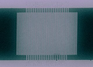
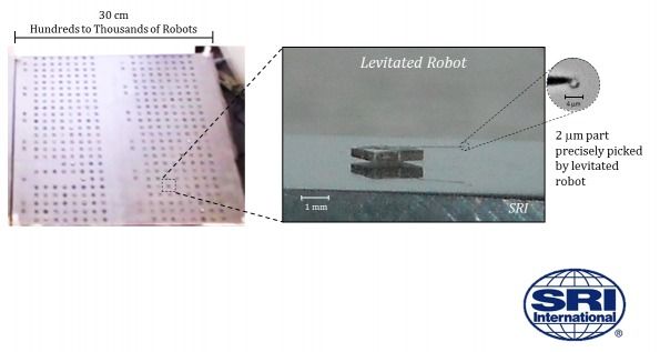
The following gallery highlights the work of five DARPA-funded projects in the program. The slides describe an atomic calligraphy technique for 2D atomic printing, a manufacturing method for producing high-frequency “Nanolitz” wires, the construction of pop-up sensors for laparoscopy, and a conjunct effort to use micro-robotics to build the assemblers of nanodevices.