Um nova “tatuagem eletrônica”, desenvolvido pela Universidade de Tel Aviv, que pode medir a atividade de pesquisadores células musculares e nervosas está pronta para revolucionar a medicina, reabilitação, e até mesmo de negócios e pesquisa de marketing.
Category: nanotechnology
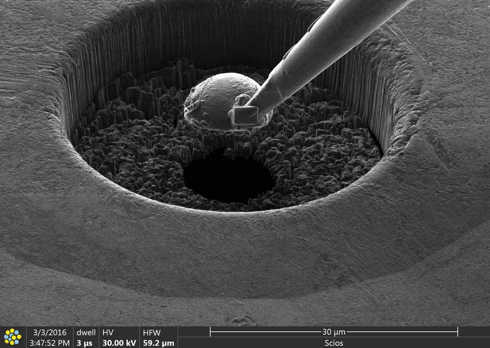
A new “nano scalpel” enables scientists at DESY to prepare samples or materials with nanometre precision while following the process with a scanning electron microscope. The Focused Ion Beam, or FIB, microscope which has now gone into service also allows a detailed view of the inner structure of materials. The device was purchased by the University of Bayreuth, as part of a joint research project on the DESY campus funded by the Federal Ministry of Research. The FIB will be operated at the DESY NanoLab jointly with the University of Bayreuth.
“The microscope is not only able to examine microscopic defects, cracks or point-like corrosion sites underneath the surfaces of materials, but also to machine the surface of samples with extremely high precision, on a nanometre scale,” explains Maxim Bykov, project scientist from the University of Bayreuth. A nanometre is a millionth of a millimetre. The ion beam can be used to remove material as though it were a microscopic milling machine; as a result, the combined ion beam and electron microscope is particularly interesting for a wide range of applications in nanotechnology, materials science and biology.
“Apart from examining the structure of materials, the ability of the ion beam to remove material also leads to a wide range of different applications,” says Natalia Dubrovinskaia who is a professor at the University of Bayreuth and in charge of the joint research project (No. 05K13WC3). One example is the preparation of tiny diamond anvils, which are used to hold samples during ultra high-pressure experiments. The diamonds used for this are so small that there is no other way of preparing them. The ion beam microscope allows so-called double-staged diamond anvil cells to be prepared with nanometre precision. The ultra high-pressure experiments are carried out at DESY’s Extreme Conditions Beamline (ECB) P02.2, headed by DESY scientist Hanns-Peter Liermann.
Faster and better method around Q-dots development which ultimately extends the quality of Quantum Dots plus mass production of Q-Dots is much faster through this new method. Hoping this causes the costs of new cameras, phone displays, monitors/ video displays are now able to be created more cheaply and in larger quantities.
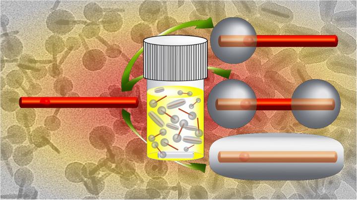
Materials researchers at North Carolina State University have fine-tuned a technique that enables them to apply precisely controlled silica coatings to quantum dot nanorods in a day — up to 21 times faster than previous methods. In addition to saving time, the advance means the quantum dots are less likely to degrade, preserving their advantageous optical properties.
Quantum dots are nanoscale semiconductor materials whose small size cause them to have electron energy levels that differ from larger-scale versions of the same material. By controlling the size of the quantum dots, researchers can control the relevant energy levels — and those energy levels give quantum dots novel optical properties. These characteristics make quantum dots promising for applications such as opto-electronics and display technologies.
But quantum dots are surrounded by ligands, which are organic molecules that are sensitive to heat. If the ligands are damaged, the optical properties of the quantum dots suffer.
To truly reach a fully connected world/ singularity we have to move tech into more and more bio-computing world. I do believe QC will assist us in getting the fundamental infrastructure we need for singularity.
We already must deal with computers too much rather than too little, and there is already lots of advanced computing done also for example in materials science and nanotechnology, for example molecular dynamics (MD) and Monte Carlo simulations.[2] The molecular biologist’s programs for predicting protein folding can also count as nanotechnology. Nevertheless, all of our previous articles concluded that we need more computing, and several mentioned statistics. This would sound predictable if coming from a statistical physicist with a background in computing, advertising his skills. However, we mean a more efficient computing rather than simply more.
We started the type of computing we do only recently and for reasons not yet mentioned: Given complex nano-micro compounds, materials’ characterization is difficult due to the three-dimensional complexity of the structures. We originally integrated image analysis with simulation in order to derive 3D structure from 2D images (SEM) and projections (TEM).[3,4] The most fruitful result was however the insight into how easy it is to create adaptable software that analyzes images and keeps track of all the data, calculating anything desired such as comparisons with numerical simulations, all in one integrated system.[5,6] Many of the previously discussed issues, for example error reporting, are thereby basically already automatically solved!
Adapting software sounds prohibitively difficult: Who in my lab can modify software? Nowadays everybody! Today, programming is done partially graphically, for example with LabView™, where no programming language appears anymore. We work with Mathematica and therefore with programming code, but we mostly just download parts of code and adapt them playfully until they behave as desired. To whomever such does not count as the ability to program, we cannot program!
Nice.
Abstract: Researchers have developed a way to use less platinum in chemical reactions commonly used in the clean energy, green chemicals, and automotive industries, according to a paper in Science.
Led by the University of New Mexico in collaboration with Washington State University, the researchers developed a unique approach for trapping platinum atoms that improves the efficiency and stability of the reactions.
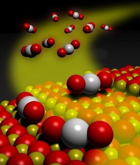
Platinum is used as a catalyst in many clean energy processes, including in catalytic converters and fuel cells. The precious metal facilitates chemical reactions for many commonly used products and processes, such as converting poisonous carbon monoxide to less harmful carbon dioxide in catalytic converters.
Aalto University scientists have broken the world record by fourteen fold in the energy resolution of thermal photodetection.
The record was made using a partially superconducting microwave detector. The discovery may lead to ultrasensitive cameras and accessories for the emerging quantum computer.
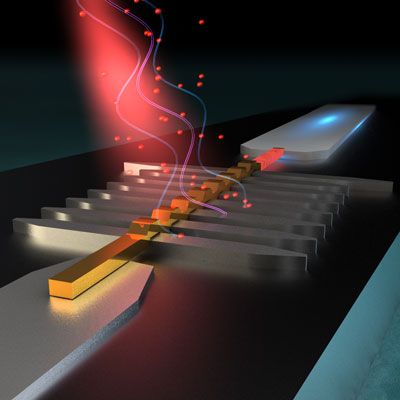
Figure 1: Artistic image of a hybrid superconductor-metal microwave detector. (Image: Ella Maru Sudio)
The first of the two key enabling developments is the new detector design consisting of tiny pieces of superconducting aluminum and a golden nanowire. This design guarantees both efficient absorption of incoming photons and very sensitive readout. The whole detector is smaller than a single human blood cell.
Robots so small they can enter the bloodstream and perform surgeries are one step closer, a research team from Monash University has discovered.
Led by Dr Zhe Liu, the Monash Engineering team has focused on graphene oxide — which is a single atom thick — as an effective shape memory material.
Graphene has captured world scientific and industrial interest for its miracle properties, with potential applications across energy, medicine, and even biomedical nano-robots.
Nearly 1,000 times thinner than a human hair, nanowires can only be understood with quantum mechanics. Using quantum models, physicists from Michigan Technological University have figured out what drives the efficiency of a silicon-germanium (Si-Ge) core-shell nanowire transistor.
Core-Shell Nanowires
The study, published last week in Nano Letters, focuses on the quantum tunneling in a core-shell nanowire structure. Ranjit Pati, a professor of physics at Michigan Tech, led the work along with his graduate students Kamal Dhungana and Meghnath Jaishi.