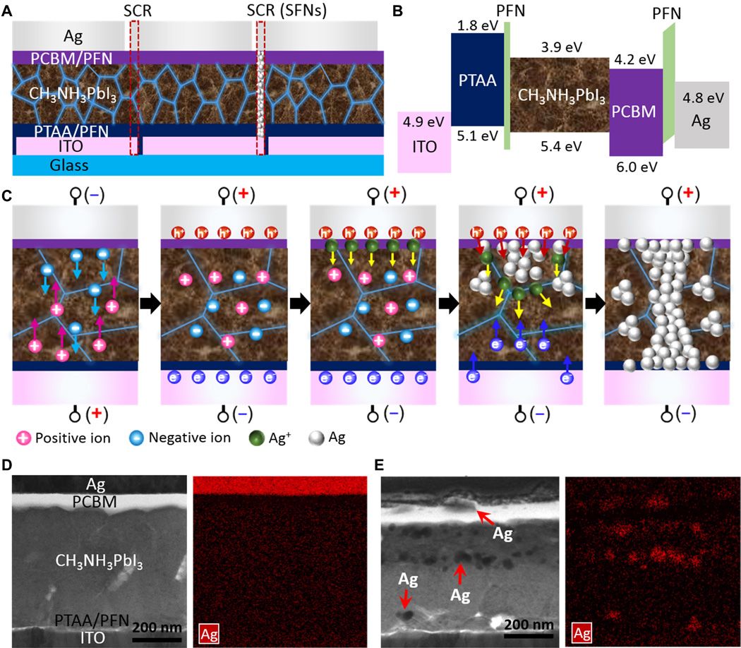
Realizing industrial-scale, large-area photovoltaic modules without any considerable performance losses compared with the performance of laboratory-scale, small-area perovskite solar cells (PSCs) has been a challenge for practical applications of PSCs. Highly sophisticated patterning processes for achieving series connections, typically fabricated using printing or laser-scribing techniques, cause unexpected efficiency drops and require complicated manufacturing processes. We successfully fabricated high-efficiency, large-area PSC modules using a new electrochemical patterning process. The intrinsic ion-conducting features of perovskites enabled us to create metal-filamentary nanoelectrodes to facilitate the monolithic serial interconnections of PSC modules. By fabricating planar-type PSC modules through low-temperature annealing and all-solution processing, we demonstrated a notably high module efficiency of 14.0% for a total area of 9.06 cm with a high geometric fill factor of 94.1%.
The unprecedented features of organic-inorganic hybrid perovskite semiconductors, which allow low-temperature crystal film growth from their precursor solutions, have greatly promoted both scientific and technological revolutions in a wide range of fields within electronics (1, 2). The advent of organolead trihalide perovskite semiconductors as light harvesters has resulted in the fastest-advancing solar technology to date, with an extremely rapid rise in power conversion efficiency (PCE) from 3.8 to 22.1% over just a few years (3–6). In addition to recent remarkable breakthroughs in addressing the instability of these devices, which has been considered the greatest challenge toward commercialization due to their intrinsic properties vulnerable to oxygen and moisture, pioneering researchers have begun fabricating large-area devices for their ultimate application (7–16).
