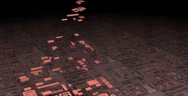
Open the hood of just about any electronic gadget and you probably will find printed circuit boards (PCBs)—most often in a leaf-green color—studded with processing, memory, data-relaying, graphics, and other types of chips and components, all interconnected with a labyrinth of finely embossed wiring. By challenging the technology community to integrate the collective functions hosted by an entire PCB onto a device approaching the size of a single chip, DARPA’s newest program is making a bid to usher in a fresh dimension of technology miniaturization.
“We are trying to push the massive amount of integration you typically get on a printed circuit board down into an even more compact format,” said Dr. Daniel Green, manager of the new program, whose acronym, “CHIPS,” is itself a typographic feat of miniaturization; the program’s full name is the Common Heterogeneous Integration and Intellectual Property (IP) Reuse Strategies Program. “It’s not just a fun acronym,” Green said. “The program is all about devising a physical library of component chips, or chiplets, that we can assemble in a modular fashion.”
A primary driver of CHIPS is to develop a novel, industry-friendly architectural strategy for designing and building new generations of microsystems in which the time and energy it takes to move signals—that is, data—between chips is reduced by factors of tens or even hundreds. “This is increasingly important for the data-intensive processing that we have to do as the data sets we are dealing with get bigger and bigger,” Green said. Although the program does not specify applications, the new architectural strategy at the program’s heart could open new routes to computational efficiencies required for such feats as identifying objects and actions in real-time video feeds, real-time language translation, and coordinating motion on-the-fly among swarms of fast-moving unmanned aerial vehicles (UAVs).
