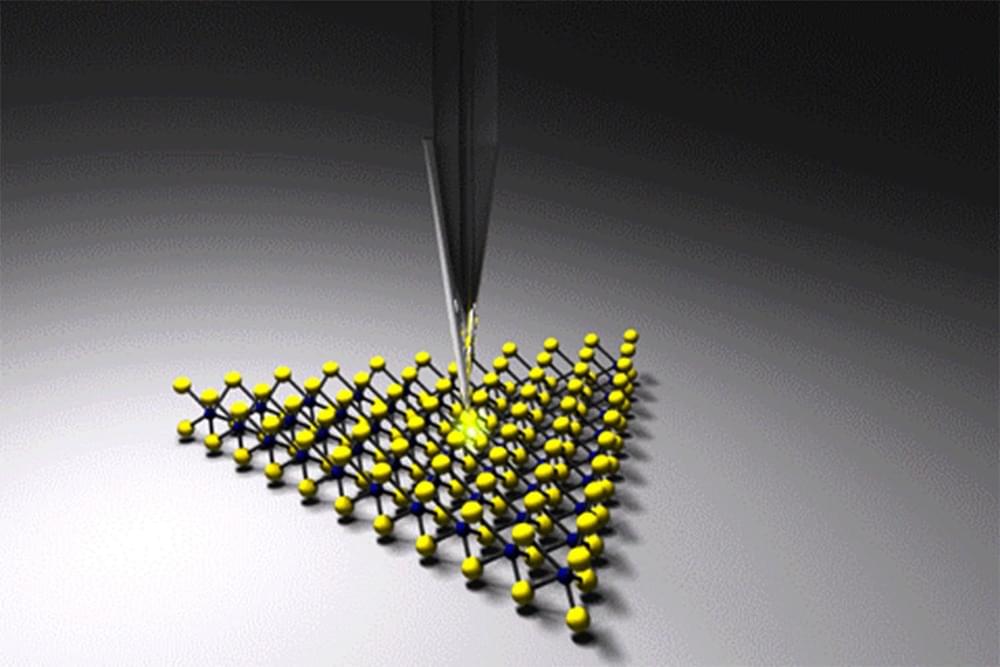
“It is like using your thumb to control the water spray from a hose,” said Ming Liu, associate professor in UC Riverside’s Marlan. “You know how to get the desired spraying pattern by changing the thumb position, and likewise, in the experiment, we read the light pattern to retrieve the details of the object blocking the five nm-sized light nozzles.”
The light is then focused into a spectrometer, where it forms a tiny ring shape. The researchers can formulate the absorption and scattering images with colors by scanning the probe over an area and recording two spectra for each pixel.
The team expects the new nano-imaging technology can be an important tool to help the semiconductor industry make uniform nanomaterials with consistent properties for use in electronic devices. The new full-color nano-imaging technique could also be used to improve understanding of catalysis, quantum optics, and nanoelectronics.
